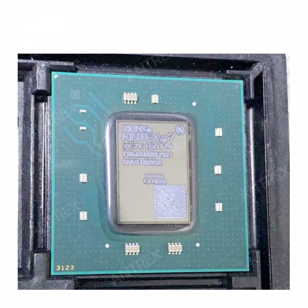

XC7K410T-L2FFG676I
IC FPGA 400 I/O 676FCBGA
- メーカー
- AMD
- 製品カテゴリ
- FPGA - フィールドプログラマブルゲートアレイ
- パッケージ
- 676-BBGA, FCBGA
- 在庫
- 1,479 pcs
- 供給状況
- 現在の数量は確認が必要です。
製品属性
| メーカー | AMD |
|---|---|
| 製品カテゴリ | FPGA - フィールドプログラマブルゲートアレイ |
| Mounting Type | Surface Mount |
| Operating Temperature | -40°C ~ 100°C (TJ) |
| Package | Tray |
| Product status | Active |
| Series | Kintex®-7 |
| Supplier Device Package | 676-FCBGA (27x27) |
| Voltage - Supply | 0.97V ~ 1.03V |
| データシート | データシート PDF を表示 |
調達概要
XC7K410T-L2FFG676I の主要な供給・購買情報です。
Antrex Electronicsを選ぶ理由
確認済みの調達、検査、国際調達要件に対して独立系ディストリビューションのサポートを提供します。
独立系ディストリビューションサポート
生産および調達要件に対応し、供給不足品、製造中止品、入手困難な電子部品の調達を支援します。
トレーサビリティ確認
注文確定前に、ラベル、ロット、デートコード、および利用可能なサプライチェーン書類を確認できます。
検査・試験
必要に応じて、外観検査、X線検査、第三者試験のサポートを手配できます。
グローバル調達サポート
OEM、EMS、ディストリビューターの国際調達要件に対応し、単品部品からBOM案件までサポートします。
認証・検証サポート
電子部品調達向けに品質管理、トレーサビリティ確認、検査サポートを提供します。


XC7K410T-L2FFG676I の詳細説明
Product Overview
The XC7K410T-L2FFG676I from AMD is a Kintex®-7 field programmable gate array (FPGA) in a 676-ball surface-mount package. The device includes 400 I/O pins, 406,720 logic elements or cells, 31,775 LABs/CLBs, and 29,306,880 total RAM bits. The supply voltage range is 0.97 V ~ 1.03 V, and the operating temperature range is -40°C ~ 100°C (TJ). The package/case designation is 676-BBGA, FCBGA, and the device package is 676-FCBGA (27x27).
Key Features
- Kintex®-7 FPGA architecture with 406,720 logic elements or cells and 31,775 LABs/CLBs.
- Includes 29,306,880 total RAM bits for on-device memory resources.
- Offers 400 I/O pins for external device connectivity.
- Uses a 0.97 V ~ 1.03 V supply voltage.
- Rated for junction temperature operation from -40°C ~ 100°C (TJ).
- Surface-mount 676-BBGA, FCBGA package; device package 676-FCBGA (27x27).
Applications
- Embedded control logic for systems that need reconfigurable digital functions.
- Programmable interface and glue logic between digital subsystems.
- Reconfigurable digital processing subsystems using FPGA logic and internal RAM resources.
Design & Procurement Notes
Designers should confirm the board land pattern, assembly process, and thermal management for the 676-FCBGA (27x27) surface-mount package. The exact part number and package designation should be used during schematic, layout, and assembly data preparation. The 0.97 V ~ 1.03 V supply range requires power delivery and decoupling suitable for the specified voltage limits. The -40°C ~ 100°C (TJ) range should be compared against system ambient conditions and the expected junction temperature. The 400 I/O pins, 406,720 logic elements or cells, 31,775 LABs/CLBs, and 29,306,880 total RAM bits should be checked against the required pin count, logic utilization, and on-device memory needs.
その他の調達オプションを見る
メーカー、製品カテゴリ、または調達要件から引き続き部品をお探しいただけます。