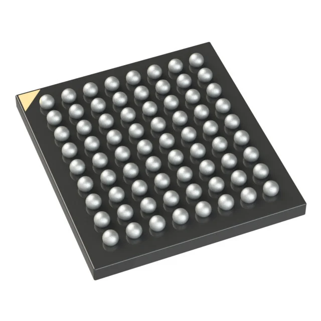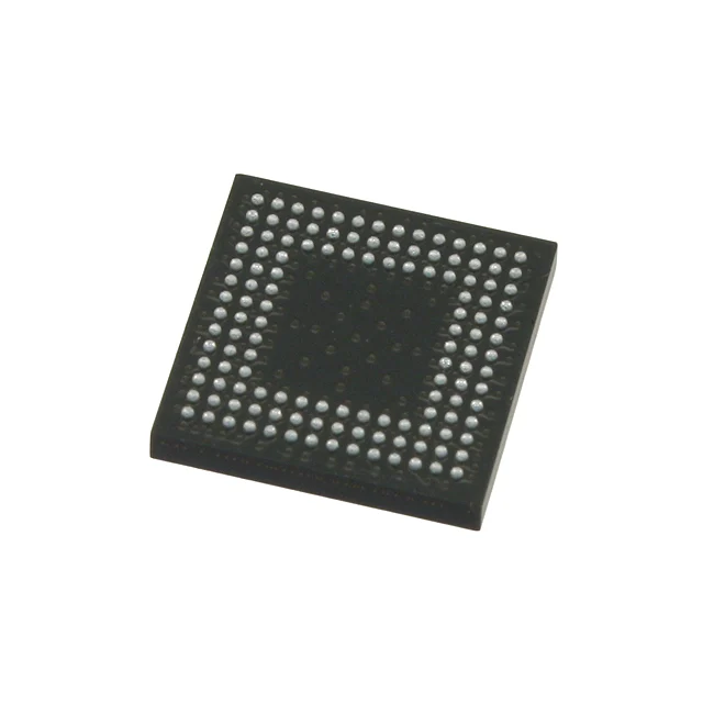

LFE2-12E-6FN484I
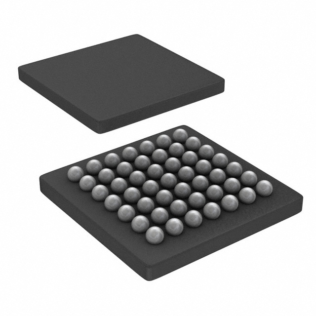
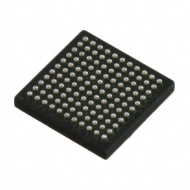
IC FPGA 297 I/O 484FBGA
- 產品分類
- FPGA - 現場可程式化閘陣列
- 封裝
- 484-BBGA
- 庫存
- 1,280 件
- 供貨狀態
- 當前數量需確認。
產品屬性
| 製造商 | Lattice Semiconductor Corporation |
|---|---|
| 產品分類 | FPGA - 現場可程式化閘陣列 |
| Mounting Type | Surface Mount |
| Operating Temperature | -40°C ~ 100°C (TJ) |
| Package | Tray |
| Product status | Active |
| Series | ECP2 |
| Supplier Device Package | 484-FPBGA (23x23) |
| Voltage - Supply | 1.14V ~ 1.26V |
| 資料表 | 查看資料表PDF |
採購概覽
LFE2-12E-6FN484I 的主要供貨及採購資訊。
為何選擇 Antrex Electronics?
為已核實的採購、檢驗及國際採購需求提供獨立分銷支援。
獨立分銷支援
支援短缺、停產及難找電子元器件的生產與採購需求。
可追溯性審查
可在訂單確認前審查標籤、批號、生產批次及現有供應鏈文件。
檢驗與測試
如有需要,可安排外觀檢查、X-ray 及第三方測試支援。
全球採購支援
支援 OEM、EMS、分銷商的國際採購需求,涵蓋單一料號及 BOM 專案。
資質與驗證支援
為電子元器件採購提供品質控制、可追溯性審查及檢驗支援。


LFE2-12E-6FN484I 詳細描述
Product Overview
The LFE2-12E-6FN484I from Lattice Semiconductor Corporation is an ECP2 field programmable gate array (FPGA) intended for embedded logic integration. It provides 12,000 logic elements or cells, 1,500 LABs/CLBs, and 226,304 total RAM bits, giving designers programmable resources for control, interface, and buffering functions within a single device. The FPGA offers 297 input/output pins and is specified for a 1.14 V to 1.26 V supply voltage. It is supplied in a 484-FPBGA (23 × 23) surface-mount package, with an operating junction temperature range of -40°C to 100°C.
Key Features
- ECP2 FPGA with 12,000 logic elements or cells and 1,500 LABs/CLBs.
- 226,304 total RAM bits for on-device data storage.
- 297 I/O pins for external interface connections.
- Supply voltage range of 1.14 V to 1.26 V.
- Surface-mount 484-FPBGA package with 23 × 23 body dimensions.
- Operating junction temperature range of -40°C to 100°C.
Applications
- Embedded control logic that implements custom state machines and peripheral interfaces.
- Interface bridging between embedded subsystems using 297 I/O and programmable logic.
- Data buffering or temporary storage within embedded designs using 226,304 total RAM bits.
- Embedded systems exposed to wide operating temperatures, where the -40°C to 100°C junction temperature range is relevant.
Design & Procurement Notes
For design planning, the 1.14 V to 1.26 V supply range should be treated as a supply voltage constraint for regulator selection, power integrity, and board-level decoupling. The 484-FPBGA (23 × 23) surface-mount package requires a footprint and routing strategy compatible with a 484-ball grid array and the 297 I/O allocation. The fixed logic and memory resources—12,000 logic elements or cells, 1,500 LABs/CLBs, and 226,304 total RAM bits—should be mapped against the target function before layout, since the device cannot be assumed to provide interface standards or qualification levels not specified. Thermal design should account for the -40°C to 100°C junction temperature limit, and procurement documentation should confirm the exact package marking and board footprint.
探索更多採購選項
可按製造商、產品分類或採購需求繼續尋找合適料號。