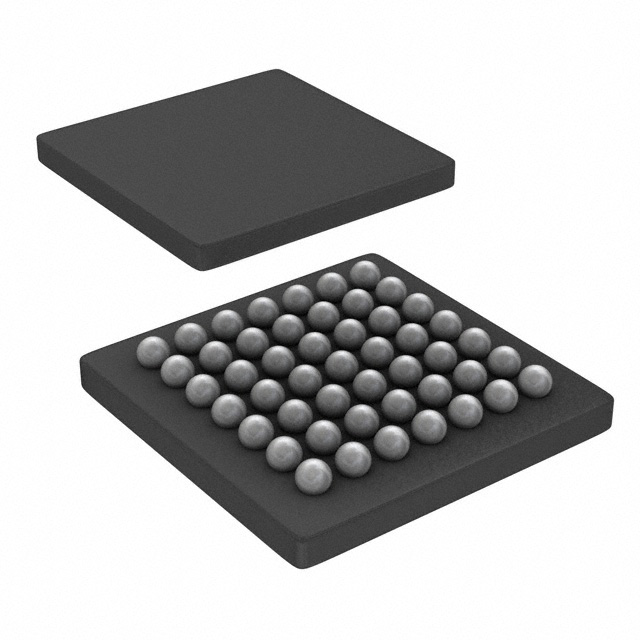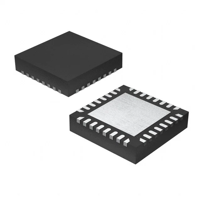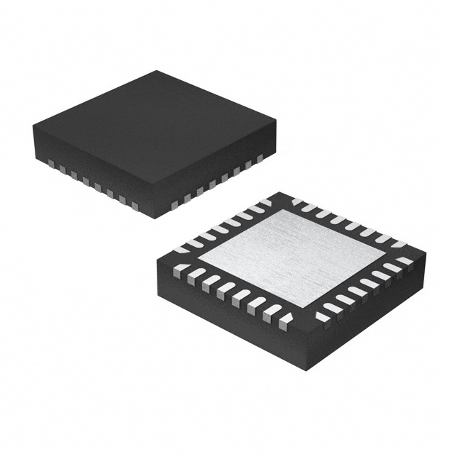
LCMXO2-640HC-4SG48C
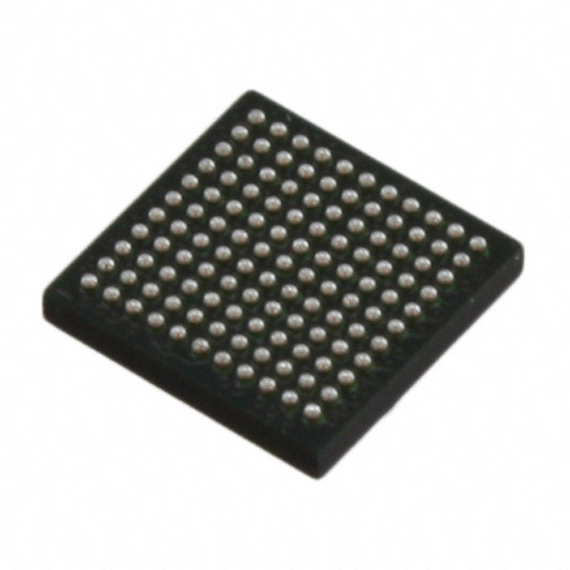
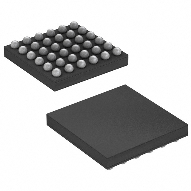
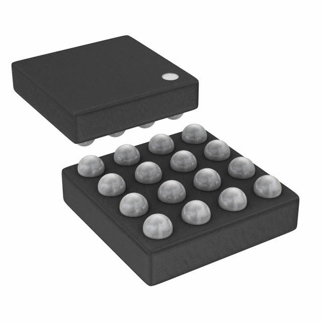
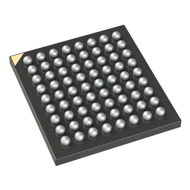
IC FPGA 40 I/O 48QFN
- 產品分類
- FPGA - 現場可程式化閘陣列
- 封裝
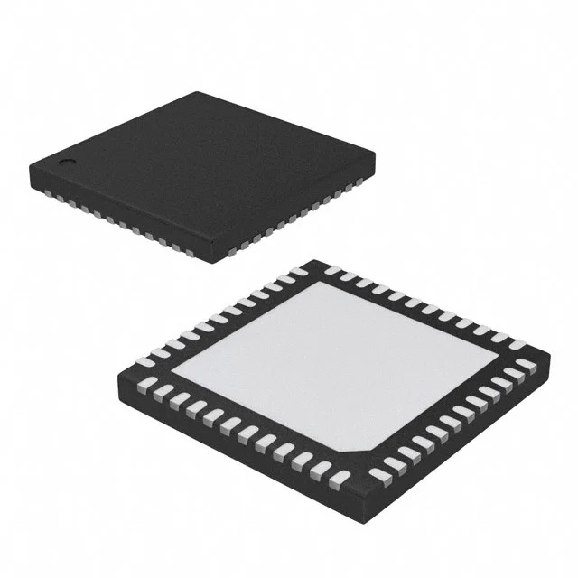
- 48-VFQFN Exposed Pad
- 庫存
- 2,802 件
- 供貨狀態
- 當前數量需確認。
產品屬性
| 製造商 | Lattice Semiconductor Corporation |
|---|---|
| 產品分類 | FPGA - 現場可程式化閘陣列 |
| Mounting Type | Surface Mount |
| Operating Temperature | 0°C ~ 85°C (TJ) |
| Package | Tray |
| Product status | Active |
| Series | MachXO2 |
| Supplier Device Package | 48-QFN (7x7) |
| Voltage - Supply | 2.375V ~ 3.465V |
| 資料表 | 查看資料表PDF |
採購概覽
LCMXO2-640HC-4SG48C 的主要供貨及採購資訊。
為何選擇 Antrex Electronics?
為已核實的採購、檢驗及國際採購需求提供獨立分銷支援。
獨立分銷支援
支援短缺、停產及難找電子元器件的生產與採購需求。
可追溯性審查
可在訂單確認前審查標籤、批號、生產批次及現有供應鏈文件。
檢驗與測試
如有需要,可安排外觀檢查、X-ray 及第三方測試支援。
全球採購支援
支援 OEM、EMS、分銷商的國際採購需求,涵蓋單一料號及 BOM 專案。
資質與驗證支援
為電子元器件採購提供品質控制、可追溯性審查及檢驗支援。


LCMXO2-640HC-4SG48C 詳細描述
Product Overview
The LCMXO2-640HC-4SG48C is a MachXO2 field programmable gate array from Lattice Semiconductor Corporation. It is packaged in a 48-VFQFN exposed pad, 48-QFN (7x7), surface-mount device package. The FPGA provides 40 I/O, 640 logic elements or cells, 80 LABs or CLBs, and 18432 total RAM bits. It operates from a 2.375V to 3.465V supply and is specified for a junction temperature range of 0°C to 85°C. This configuration supports embedded logic functions that require programmable resources, a defined I/O count, and a compact QFN footprint.
Key Features
- 40 I/O pins for external digital interfacing
- 640 logic elements or cells for programmable logic implementation
- 80 LABs or CLBs as the logic block organization
- 18432 total RAM bits for on-chip data storage
- 2.375V to 3.465V supply voltage range
- 0°C to 85°C operating junction temperature range
- 48-VFQFN exposed pad package, 48-QFN (7x7), surface mount
Applications
- Embedded control logic in general-purpose electronic assemblies
- Glue logic and signal routing between digital components
- Programmable interface adaptation for digital subsystems
- Small-scale data buffering using available on-chip RAM bits
- Compact surface-mount FPGA implementations in space-constrained boards
Design & Procurement Notes
Designers should confirm that the PCB footprint and thermal path support the 48-VFQFN exposed pad package and that the junction temperature remains within 0°C to 85°C. The system supply should remain within 2.375V to 3.465V during operation, and the 40 I/O pins should be checked against required external interfaces. Logic utilization should be evaluated against the 640 logic elements or cells, 80 LABs or CLBs, and 18432 total RAM bits before implementation. For procurement, match the exact manufacturer part number LCMXO2-640HC-4SG48C to the required package, voltage range, and temperature specification to avoid substitutions that alter footprint, electrical margin, or thermal limits.
探索更多採購選項
可按製造商、產品分類或採購需求繼續尋找合適料號。