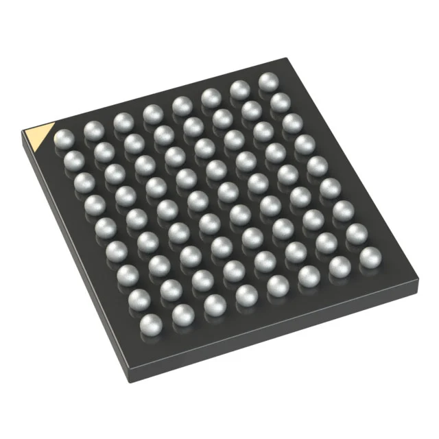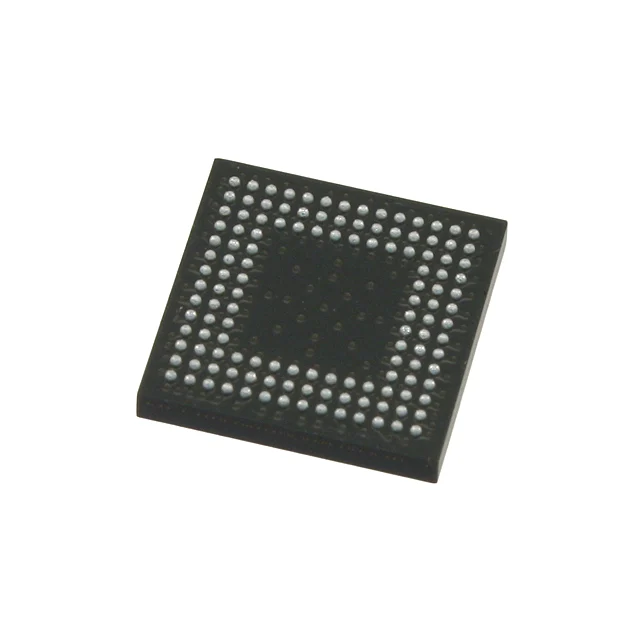
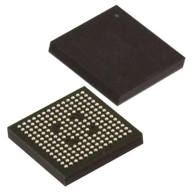
LCMXO2-4000HE-6MG184C
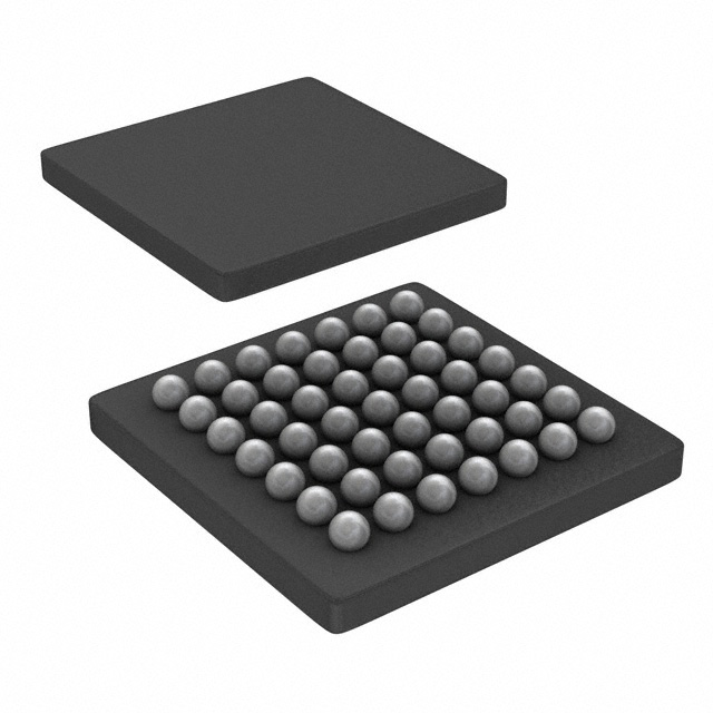
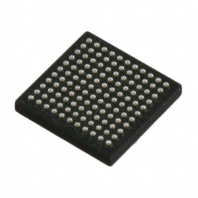
IC FPGA 150 I/O 184CSBGA
- 產品分類
- FPGA - 現場可程式化閘陣列
- 封裝
- 184-LFBGA, CSPBGA
- 庫存
- 1,312 件
- 供貨狀態
- 當前數量需確認。
產品屬性
| 製造商 | Lattice Semiconductor Corporation |
|---|---|
| 產品分類 | FPGA - 現場可程式化閘陣列 |
| Mounting Type | Surface Mount |
| Operating Temperature | 0°C ~ 85°C (TJ) |
| Package | Tray |
| Product status | Active |
| Series | MachXO2 |
| Supplier Device Package | 184-CSBGA (8x8) |
| Voltage - Supply | 1.14V ~ 1.26V |
| 資料表 | 查看資料表PDF |
採購概覽
LCMXO2-4000HE-6MG184C 的主要供貨及採購資訊。
為何選擇 Antrex Electronics?
為已核實的採購、檢驗及國際採購需求提供獨立分銷支援。
獨立分銷支援
支援短缺、停產及難找電子元器件的生產與採購需求。
可追溯性審查
可在訂單確認前審查標籤、批號、生產批次及現有供應鏈文件。
檢驗與測試
如有需要,可安排外觀檢查、X-ray 及第三方測試支援。
全球採購支援
支援 OEM、EMS、分銷商的國際採購需求,涵蓋單一料號及 BOM 專案。
資質與驗證支援
為電子元器件採購提供品質控制、可追溯性審查及檢驗支援。


LCMXO2-4000HE-6MG184C 詳細描述
Product Overview
The LCMXO2-4000HE-6MG184C from Lattice Semiconductor Corporation is a MachXO2 Field Programmable Gate Array (FPGA) for embedded programmable logic applications. It provides 4,320 logic elements or cells, 540 LABs or CLBs, and 94,208 total RAM bits, with 150 I/O connections. The device uses a 184-LFBGA, CSPBGA package with a 184-CSBGA (8x8) package designation and is intended for surface-mount assembly. The supply voltage range is 1.14 V to 1.26 V, and the operating temperature range is 0°C to 85°C at the junction (TJ).
Key Features
- 4,320 logic elements or cells for programmable logic design.
- 540 LABs or CLBs and 94,208 total RAM bits.
- 150 I/O connections for external interfacing.
- 1.14 V to 1.26 V supply voltage range.
- 0°C to 85°C operating temperature range at the junction (TJ).
- 184-LFBGA, CSPBGA package with 184-CSBGA (8x8) package designation.
- Surface-mount mounting type.
Applications
- Embedded control logic requiring custom combinational and sequential behavior.
- Peripheral interfacing and I/O expansion using the available programmable resources.
- On-chip buffering and data aggregation for embedded data paths.
Design & Procurement Notes
Designers should plan board-level power delivery around the 1.14 V to 1.26 V supply range and account for the 0°C to 85°C junction temperature limit during thermal analysis. The 184-LFBGA, CSPBGA package and 184-CSBGA (8x8) package designation should be used as the starting point for footprint, land pattern, and assembly-process planning, with surface-mount assembly considered. The 150 I/O count, 4,320 logic elements or cells, 540 LABs or CLBs, and 94,208 total RAM bits should be checked against the target logic and buffering requirements before finalizing the design.
探索更多採購選項
可按製造商、產品分類或採購需求繼續尋找合適料號。