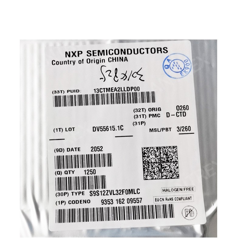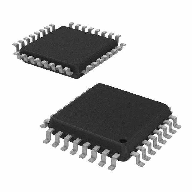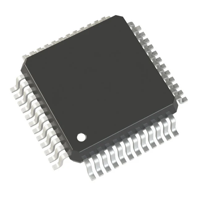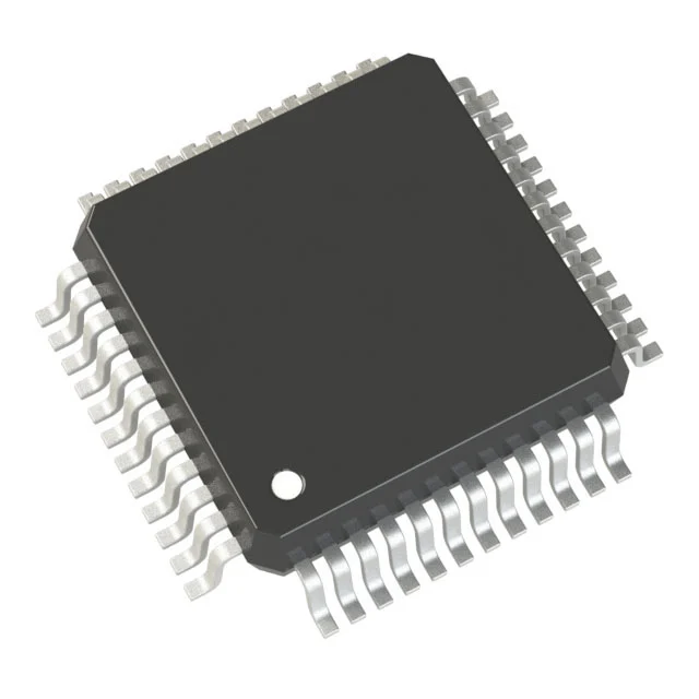
S9S12G96F0CLFR
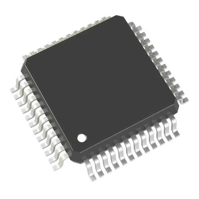
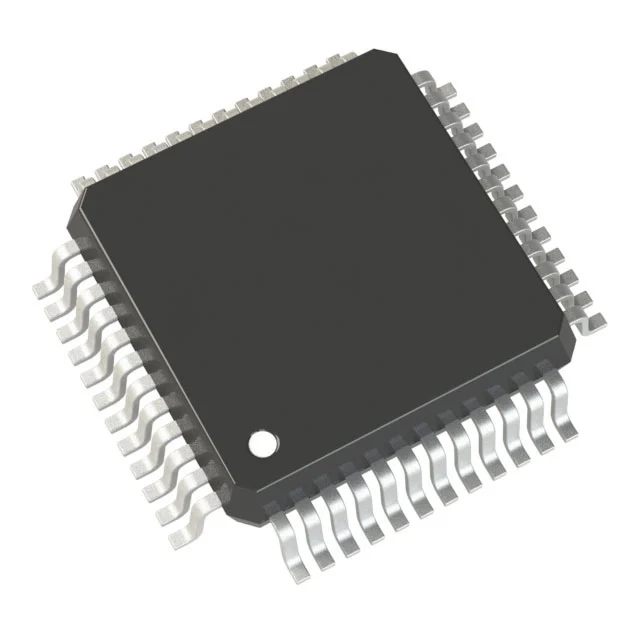
IC MCU 16BIT 96KB FLASH 48LQFP
- 製造商
- NXP USA Inc.
- 產品分類
- 微控制器 - MCU
- 封裝
- 48-LQFP
- 庫存
- 9,990 件
- 供貨狀態
- 當前數量需確認。
產品屬性
| 製造商 | NXP USA Inc. |
|---|---|
| 產品分類 | 微控制器 - MCU |
| Connectivity | CANbus, IrDA, LINbus, SCI, SPI |
| Core Processor | 12V1 |
| Core Size | 16-Bit |
| Data Converters | A/D 12x10b |
| EEPROM Size | 3K x 8 |
| Mounting Type | Surface Mount |
| Number of I/O | 40 |
| Operating Temperature | -40°C ~ 85°C (TA) |
| Oscillator Type | Internal |
| Package | Tape & Reel (TR),Cut Tape (CT) |
| Peripherals | LVD, POR, PWM, WDT |
| Product status | Active |
| Program Memory Size | 96KB (96K x 8) |
| Program Memory Type | Flash |
| RAM Size | 8K x 8 |
| Series | HCS12 |
| Speed | 25MHz |
| Supplier Device Package | 48-LQFP (7x7) |
| Voltage - Supply (Vcc/Vdd) | 3.13V ~ 5.5V |
| 資料表 | 查看資料表PDF |
採購概覽
S9S12G96F0CLFR 的主要供貨及採購資訊。
為何選擇 Antrex Electronics?
為已核實的採購、檢驗及國際採購需求提供獨立分銷支援。
獨立分銷支援
支援短缺、停產及難找電子元器件的生產與採購需求。
可追溯性審查
可在訂單確認前審查標籤、批號、生產批次及現有供應鏈文件。
檢驗與測試
如有需要,可安排外觀檢查、X-ray 及第三方測試支援。
全球採購支援
支援 OEM、EMS、分銷商的國際採購需求,涵蓋單一料號及 BOM 專案。
資質與驗證支援
為電子元器件採購提供品質控制、可追溯性審查及檢驗支援。


S9S12G96F0CLFR 詳細描述
Product Overview
The NXP USA Inc. S9S12G96F0CLFR is a 16-bit HCS12 microcontroller built around a 12V1 core and specified for operation at 25 MHz. It provides 96KB (96K x 8) FLASH program memory, 8K x 8 RAM, and 3K x 8 EEPROM within a 48-LQFP (7x7) surface-mount package. The device integrates 40 I/O points, an internal oscillator, and a 12x10-bit A/D converter, while supporting CANbus, LINbus, SCI, SPI, and IrDA communication interfaces. Peripheral blocks include PWM, LVD, POR, and WDT. The supply voltage range is 3.13V to 5.5V, and the operating temperature range is -40°C to 85°C (TA).
Key Features
- 16-bit 12V1 HCS12 core with a 25 MHz speed.
- 96KB (96K x 8) FLASH, 8K x 8 RAM, and 3K x 8 EEPROM.
- 40 I/O points in a 48-LQFP (7x7) surface-mount package.
- Communication interfaces include CANbus, LINbus, SCI, SPI, and IrDA.
- 12x10-bit A/D converter and internal oscillator.
- On-chip peripherals include PWM, LVD, POR, and WDT.
- Operating supply voltage of 3.13V to 5.5V and temperature range of -40°C to 85°C (TA).
Applications
- Embedded control nodes using CANbus or LINbus communication.
- Analog sensor acquisition and measurement using the 12x10-bit A/D converter.
- Serial communication endpoints using SCI, SPI, or IrDA interfaces.
- Control applications using PWM outputs and WDT operation.
Design & Procurement Notes
For board design, the 48-LQFP (7x7) surface-mount package requires routing for 40 I/O points. The 3.13V to 5.5V supply range should be evaluated against the system power rail, while the -40°C to 85°C (TA) range should be checked for the intended operating environment. Memory resources consist of 96KB (96K x 8) FLASH, 8K x 8 RAM, and 3K x 8 EEPROM, which are relevant for firmware size, runtime data, and stored parameters. The internal oscillator reduces external timing component needs, but the 25 MHz speed and available CANbus, LINbus, SCI, SPI, IrDA, PWM, LVD, POR, and WDT functions should be matched to the selected control and communication requirements.
探索更多採購選項
可按製造商、產品分類或採購需求繼續尋找合適料號。