SI5340B-D-GM
IC JITTER ATTENUATOR/MULTIPLEXER
- Manufacturer
- Skyworks Solutions Inc.
- Product Category
- Clock Generators, PLLs, Frequency Synthesizers
- Package
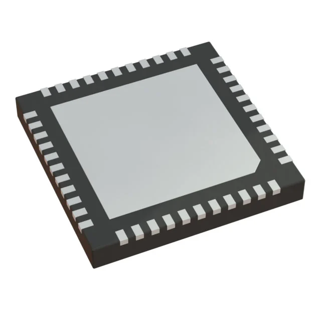
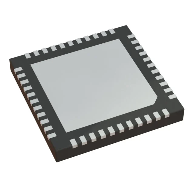
- 44-VFQFN Exposed Pad
- Stock
- 1,564 pcs
- Availability
- Current quantity subject to confirmation.
Product Attributes
| Manufacturer | Skyworks Solutions Inc. |
|---|---|
| Product Category | Clock Generators, PLLs, Frequency Synthesizers |
| Differential - Input:Output | Yes/Yes |
| Divider/Multiplier | Yes/No |
| Frequency - Max | 350MHz |
| Input | LVCMOS, LVDS, LVPECL, Crystal |
| Mounting Type | Surface Mount |
| Number of Circuits | 1 |
| Operating Temperature | -40°C ~ 85°C |
| Output | CML, HCSL, LVCMOS, LVDS, LVPECL |
| Package | Tray |
| PLL | Yes |
| Product status | Active |
| Ratio - Input:Output | 4:4 |
| Supplier Device Package | 44-QFN (7x7) |
| Voltage - Supply | 1.71V ~ 3.47V |
| Datasheet | View Datasheet PDF |
Procurement Snapshot
Key supply and purchasing information for SI5340B-D-GM.
Why Source from Antrex Electronics?
Independent distribution support for verified sourcing, inspection and international procurement requirements.
Independent Distribution Support
Shortage, obsolete and hard-to-find component sourcing for production and procurement requirements.
Traceability Review
Label, lot, date code and available supply-chain documentation can be reviewed before order confirmation.
Inspection & Testing
Visual inspection, X-ray and third-party testing support can be arranged when required.
Global Procurement Support
Support for OEM, EMS, distributors and international sourcing requirements across individual parts and BOM projects.
Credentials & Verification Support
Quality controls, traceability review and inspection support for electronic component sourcing.


Detailed Description for SI5340B-D-GM
Product Overview
The SI5340B-D-GM from Skyworks Solutions Inc. is a surface-mount clock and timing integrated circuit that combines jitter attenuation and multiplexing functions in a 44-VFQFN exposed-pad package. It supports a PLL, accepts LVCMOS, LVDS, LVPECL, and crystal inputs, and provides CML, HCSL, LVCMOS, LVDS, and LVPECL outputs. The device supports a maximum frequency of 350 MHz and a supply range of 1.71 V to 3.47 V, with operation from -40°C to 85°C. Its 4:4 input-to-output ratio and differential input/output capability support clock distribution architectures with multiple input sources and output formats.
Key Features
- Jitter attenuator and multiplexer function for clock and timing paths
- PLL included, with differential input and output support
- Input options include LVCMOS, LVDS, LVPECL, and crystal
- Output options include CML, HCSL, LVCMOS, LVDS, and LVPECL
- 4:4 input-to-output ratio with a maximum frequency of 350 MHz
- Supply range of 1.71 V to 3.47 V and operating temperature range of -40°C to 85°C
- Surface-mount 44-QFN (7x7) package with exposed pad
Applications
- Clock selection and distribution in communications infrastructure equipment
- Timing synchronization on server, storage, and backplane boards
- Reference clock routing for test and measurement equipment
- Mixed-logic clock delivery in embedded processing boards
Design & Procurement Notes
Designers should confirm that available clock sources and downstream loads match the supported input and output logic families, including LVCMOS, LVDS, LVPECL, and crystal inputs, and CML, HCSL, LVCMOS, LVDS, and LVPECL outputs. The 4:4 input-to-output ratio and single circuit should be considered when planning the clock tree, source selection, output loading, and differential pair requirements. Board layout should address the 44-QFN (7x7) exposed pad, surface-mount land pattern, and thermal dissipation under the -40°C to 85°C operating range. The 1.71 V to 3.47 V supply range should be checked against local power rails and voltage margining.
Explore More Sourcing Options
Continue sourcing by manufacturer, product category or procurement requirement.