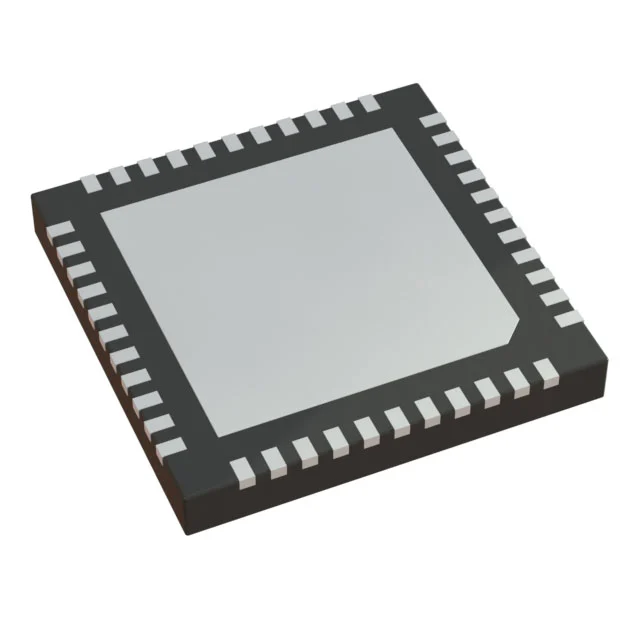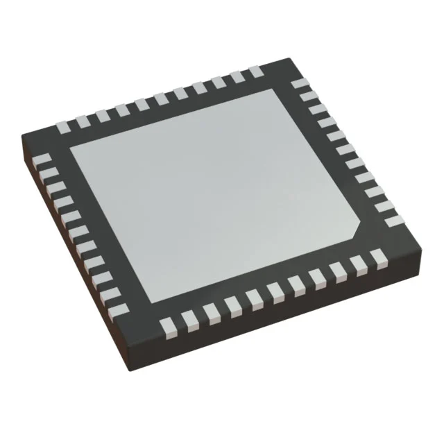
SI5340B-D-GM
IC JITTER ATTENUATOR/MULTIPLEXER
- 製品カテゴリ
- クロックジェネレータ、PLL、周波数シンセサイザ
- パッケージ
- 44-VFQFN Exposed Pad
- 在庫
- 1,564 pcs
- 供給状況
- 現在の数量は確認が必要です。
製品属性
| メーカー | Skyworks Solutions Inc. |
|---|---|
| 製品カテゴリ | クロックジェネレータ、PLL、周波数シンセサイザ |
| Differential - Input:Output | Yes/Yes |
| Divider/Multiplier | Yes/No |
| Frequency - Max | 350MHz |
| Input | LVCMOS, LVDS, LVPECL, Crystal |
| Mounting Type | Surface Mount |
| Number of Circuits | 1 |
| Operating Temperature | -40°C ~ 85°C |
| Output | CML, HCSL, LVCMOS, LVDS, LVPECL |
| Package | Tray |
| PLL | Yes |
| Product status | Active |
| Ratio - Input:Output | 4:4 |
| Supplier Device Package | 44-QFN (7x7) |
| Voltage - Supply | 1.71V ~ 3.47V |
| データシート | データシート PDF を表示 |
調達概要
SI5340B-D-GM の主要な供給・購買情報です。
Antrex Electronicsを選ぶ理由
確認済みの調達、検査、国際調達要件に対して独立系ディストリビューションのサポートを提供します。
独立系ディストリビューションサポート
生産および調達要件に対応し、供給不足品、製造中止品、入手困難な電子部品の調達を支援します。
トレーサビリティ確認
注文確定前に、ラベル、ロット、デートコード、および利用可能なサプライチェーン書類を確認できます。
検査・試験
必要に応じて、外観検査、X線検査、第三者試験のサポートを手配できます。
グローバル調達サポート
OEM、EMS、ディストリビューターの国際調達要件に対応し、単品部品からBOM案件までサポートします。
認証・検証サポート
電子部品調達向けに品質管理、トレーサビリティ確認、検査サポートを提供します。


SI5340B-D-GM の詳細説明
Product Overview
The SI5340B-D-GM from Skyworks Solutions Inc. is a surface-mount clock and timing integrated circuit that combines jitter attenuation and multiplexing functions in a 44-VFQFN exposed-pad package. It supports a PLL, accepts LVCMOS, LVDS, LVPECL, and crystal inputs, and provides CML, HCSL, LVCMOS, LVDS, and LVPECL outputs. The device supports a maximum frequency of 350 MHz and a supply range of 1.71 V to 3.47 V, with operation from -40°C to 85°C. Its 4:4 input-to-output ratio and differential input/output capability support clock distribution architectures with multiple input sources and output formats.
Key Features
- Jitter attenuator and multiplexer function for clock and timing paths
- PLL included, with differential input and output support
- Input options include LVCMOS, LVDS, LVPECL, and crystal
- Output options include CML, HCSL, LVCMOS, LVDS, and LVPECL
- 4:4 input-to-output ratio with a maximum frequency of 350 MHz
- Supply range of 1.71 V to 3.47 V and operating temperature range of -40°C to 85°C
- Surface-mount 44-QFN (7x7) package with exposed pad
Applications
- Clock selection and distribution in communications infrastructure equipment
- Timing synchronization on server, storage, and backplane boards
- Reference clock routing for test and measurement equipment
- Mixed-logic clock delivery in embedded processing boards
Design & Procurement Notes
Designers should confirm that available clock sources and downstream loads match the supported input and output logic families, including LVCMOS, LVDS, LVPECL, and crystal inputs, and CML, HCSL, LVCMOS, LVDS, and LVPECL outputs. The 4:4 input-to-output ratio and single circuit should be considered when planning the clock tree, source selection, output loading, and differential pair requirements. Board layout should address the 44-QFN (7x7) exposed pad, surface-mount land pattern, and thermal dissipation under the -40°C to 85°C operating range. The 1.71 V to 3.47 V supply range should be checked against local power rails and voltage margining.
その他の調達オプションを見る
メーカー、製品カテゴリ、または調達要件から引き続き部品をお探しいただけます。