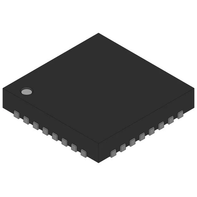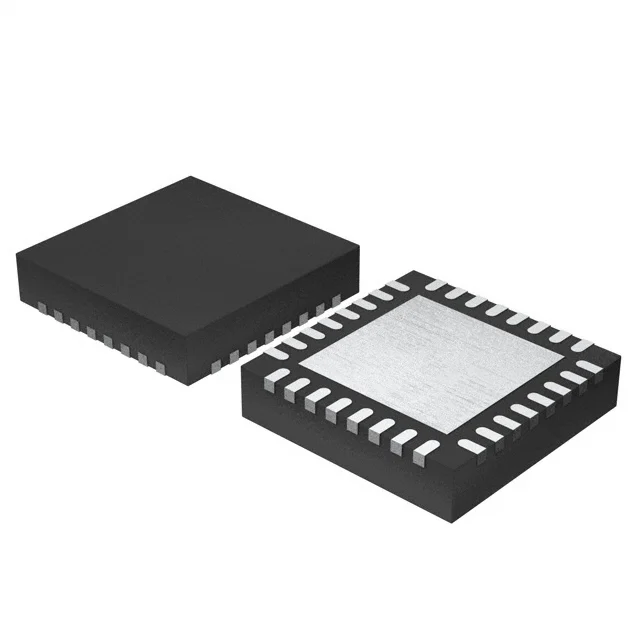
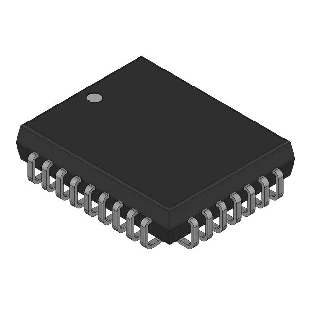
CY7C9915JXI-1
IC FANOUT BUFFER 32PLCC
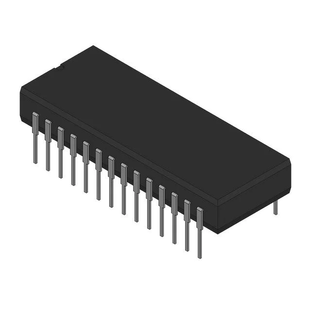
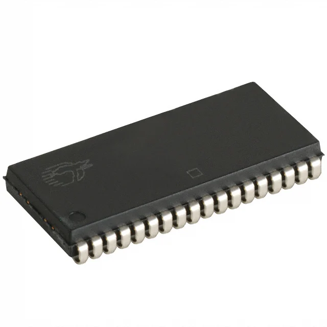
Quick Answer: The Cypress Semiconductor Corp CY7C9915JXI-1 is a surface-mount clock distribution device packaged in a 32-LCC (J-Lead) case.
- Manufacturer
- Cypress Semiconductor Corp
- Product Category
- Clock Generators, PLLs, Frequency Synthesizers
- Package
- 32-LCC (J-Lead)
- Stock
- 3,297 pcs
- Availability
- Current quantity subject to confirmation.
Product Attributes
| Manufacturer | Cypress Semiconductor Corp |
|---|---|
| Product Category | Clock Generators, PLLs, Frequency Synthesizers |
| Differential - Input:Output | No/No |
| Divider/Multiplier | Yes/Yes |
| Frequency - Max | 150MHz |
| Input | LVCMOS, LVTTL |
| Mounting Type | Surface Mount |
| Number of Circuits | 1 |
| Operating Temperature | -40°C ~ 85°C |
| Output | LVTTL |
| Package | Bulk |
| PLL | Yes |
| Product status | Obsolete |
| Ratio - Input:Output | 1:8 |
| Series | RoboClock™ |
| Supplier Device Package | 32-PLCC (11.43x13.97) |
| Type | Fanout Buffer (Distribution), Zero Delay Buffer |
| Voltage - Supply | 2.97V ~ 3.63V |
| Datasheet | View Datasheet PDF |
Procurement Snapshot
Key supply and purchasing information for CY7C9915JXI-1.
Why Source from Antrex Electronics?
Independent distribution support for verified sourcing, inspection and international procurement requirements.
Independent Distribution Support
Shortage, obsolete and hard-to-find component sourcing for production and procurement requirements.
Traceability Review
Label, lot, date code and available supply-chain documentation can be reviewed before order confirmation.
Inspection & Testing
Visual inspection, X-ray and third-party testing support can be arranged when required.
Global Procurement Support
Support for OEM, EMS, distributors and international sourcing requirements across individual parts and BOM projects.
Credentials & Verification Support
Quality controls, traceability review and inspection support for electronic component sourcing.


Detailed Description for CY7C9915JXI-1
Product Overview
The Cypress Semiconductor Corp CY7C9915JXI-1 is a surface-mount clock distribution device packaged in a 32-LCC (J-Lead) case. It functions as a fanout buffer and zero delay buffer with an integrated PLL, accepting LVCMOS or LVTTL inputs and providing LVTTL outputs. The device supports a maximum frequency of 150 MHz and a 1:8 input-to-output ratio, with divider and multiplier capability. Supply voltage operation is specified from 2.97 V to 3.63 V, and the operating temperature range is -40°C to 85°C.
Key Features
- Type: Fanout Buffer (Distribution), Zero Delay Buffer.
- Integrated PLL with divider and multiplier capability.
- Input logic family: LVCMOS, LVTTL; output logic family: LVTTL.
- 1:8 input-to-output ratio with one circuit and non-differential input/output configuration.
- Maximum operating frequency of 150 MHz.
- 2.97 V to 3.63 V supply voltage range and -40°C to 85°C operating temperature range.
- Surface-mount 32-LCC (J-Lead) package with 32-PLCC (11.43x13.97) case dimensions.
Applications
- Distribution of one clock signal to multiple LVTTL loads on a printed circuit board.
- Phase alignment of a clock path when a zero-delay buffering function is required.
- Frequency synthesis or conditioning using the internal PLL divider and multiplier functions.
- Buffering of LVCMOS or LVTTL logic-level clock inputs for downstream LVTTL timing circuits.
Design & Procurement Notes
Design considerations include the non-differential LVCMOS/LVTTL input and LVTTL output compatibility, the 1:8 fanout ratio, and the 150 MHz maximum frequency. The 2.97 V to 3.63 V supply range should be checked against board power rails, while the -40°C to 85°C operating range defines the environmental envelope. The non-differential input/output configuration affects trace pairing and termination decisions. The 32-LCC (J-Lead) surface-mount package requires footprint and land pattern compatibility, with 32-PLCC (11.43x13.97) case dimensions providing the physical reference for layout.
Explore More Sourcing Options
Continue sourcing by manufacturer, product category or procurement requirement.