
CY26049ZXC-36
IC CLK/FREQ SYNTH 16TSSOP
- 제품 카테고리
- 클록 발생기, PLL 및 주파수 합성기
- 패키지
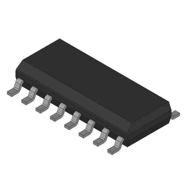
- 16-TSSOP (0.173", 4.40mm Width)
- 재고
- 5,961 개
- 공급 가능 여부
- 현재 수량은 확인이 필요합니다.
제품 특성
| 제조사 | Cypress Semiconductor Corp |
|---|---|
| 제품 카테고리 | 클록 발생기, PLL 및 주파수 합성기 |
| Differential - Input:Output | No/No |
| Divider/Multiplier | Yes/No |
| Frequency - Max | 155MHz |
| Input | Clock |
| Mounting Type | Surface Mount |
| Number of Circuits | 1 |
| Operating Temperature | 0°C ~ 70°C |
| Output | Clock |
| Package | Tube,Tube |
| PLL | Yes with Bypass |
| Product status | Obsolete |
| Ratio - Input:Output | 1:3 |
| Series | Failsafe™, PacketClock™ |
| Supplier Device Package | 16-TSSOP |
| Type | Clock/Frequency Synthesizer, Clock Generator, Fanout Distribution, Jitter Attenuator |
| Voltage - Supply | 3.15V ~ 3.45V |
| 데이터시트 | 데이터시트 PDF 보기 |
조달 개요
CY26049ZXC-36의 주요 공급 및 구매 정보입니다.
왜 Antrex Electronics인가요?
검증된 소싱, 검사 및 글로벌 조달 요구에 대해 독립 유통 지원을 제공합니다.
독립 유통 지원
생산 및 조달 요구에 맞춰 수급난, 단종 및 구하기 어려운 전자부품 소싱을 지원합니다.
추적성 검토
주문 확정 전에 라벨, Lot, Date Code 및 제공 가능한 공급망 문서를 검토할 수 있습니다.
검사 및 테스트
필요 시 외관 검사, X-ray 및 제3자 테스트 지원을 진행할 수 있습니다.
글로벌 조달 지원
OEM, EMS 및 유통업체의 국제 조달 요구를 지원하며 단일 부품부터 BOM 프로젝트까지 대응합니다.
인증 및 검증 지원
전자부품 조달을 위한 품질 관리, 추적성 검토 및 검사 지원을 제공합니다.


CY26049ZXC-36 상세 설명
Product Overview
The CY26049ZXC-36 from Cypress Semiconductor Corp is a surface-mount clock and frequency synthesis device intended for timing distribution and clock generation tasks in digital systems. It combines clock/frequency synthesizer, clock generator, fanout distribution, and jitter attenuation functions in a single 16-TSSOP package. The device accepts a clock input and provides clock outputs, with a 1:3 input-to-output ratio and a maximum frequency rating of 155MHz. A PLL with bypass is included, while the input and output interfaces are non-differential. The supply range is 3.15V to 3.45V, and the operating temperature range is 0°C to 70°C.
Key Features
- Integrated clock/frequency synthesizer, clock generator, fanout distribution, and jitter attenuator functions.
- PLL with bypass capability.
- Single circuit with clock input and clock output, using a 1:3 input-to-output ratio.
- Maximum frequency rating of 155MHz.
- Non-differential input and output interfaces.
- 3.15V to 3.45V supply range and 0°C to 70°C operating range.
- Surface-mount 16-TSSOP package, 0.173 inch / 4.40mm width.
Applications
- Clock distribution to several synchronous logic blocks on a PCB.
- Jitter attenuation in clock paths feeding synchronous digital subsystems.
- Clock regeneration for digital equipment requiring a common timing reference.
Design & Procurement Notes
For CY26049ZXC-36, check that the board uses non-differential clock input and output interfaces, as the device has non-differential input and output. Confirm that the timing architecture is compatible with the 1:3 input-to-output ratio and that all required clock signals remain within the 155MHz maximum frequency. The 3.15V to 3.45V supply range and 0°C to 70°C operating range should match the system power rail and ambient conditions. The surface-mount 16-TSSOP package, 0.173 inch / 4.40mm width, should be considered during footprint layout, soldering process selection, and mechanical clearance planning. Review manufacturer technical documentation for pin assignments, configuration, and detailed timing guidance.
더 많은 소싱 옵션 보기
제조사, 제품 카테고리 또는 조달 요구사항별로 계속 소싱할 수 있습니다.