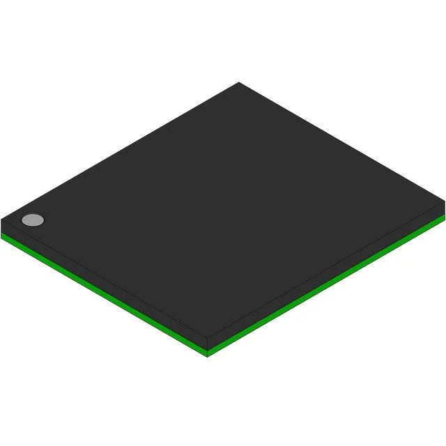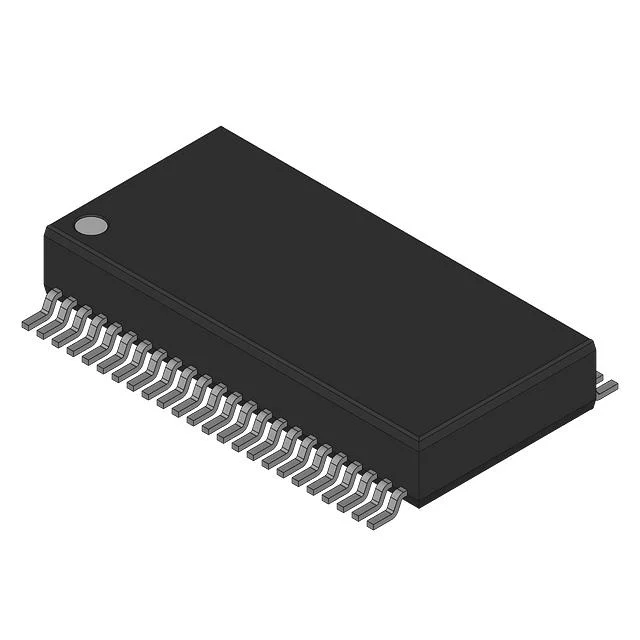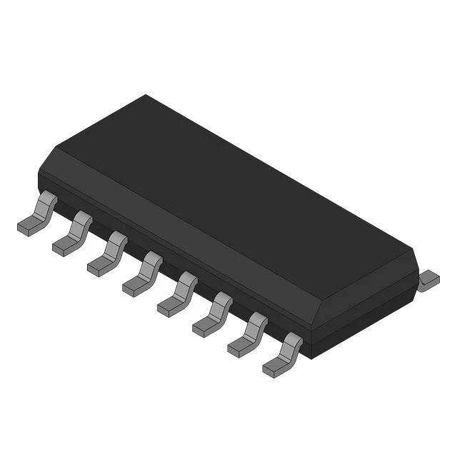

CY26049ZXC-36
IC CLK/FREQ SYNTH 16TSSOP
- 製品カテゴリ
- クロックジェネレータ、PLL、周波数シンセサイザ
- パッケージ
- 16-TSSOP (0.173", 4.40mm Width)
- 在庫
- 5,961 pcs
- 供給状況
- 現在の数量は確認が必要です。
製品属性
| メーカー | Cypress Semiconductor Corp |
|---|---|
| 製品カテゴリ | クロックジェネレータ、PLL、周波数シンセサイザ |
| Differential - Input:Output | No/No |
| Divider/Multiplier | Yes/No |
| Frequency - Max | 155MHz |
| Input | Clock |
| Mounting Type | Surface Mount |
| Number of Circuits | 1 |
| Operating Temperature | 0°C ~ 70°C |
| Output | Clock |
| Package | Tube,Tube |
| PLL | Yes with Bypass |
| Product status | Obsolete |
| Ratio - Input:Output | 1:3 |
| Series | Failsafe™, PacketClock™ |
| Supplier Device Package | 16-TSSOP |
| Type | Clock/Frequency Synthesizer, Clock Generator, Fanout Distribution, Jitter Attenuator |
| Voltage - Supply | 3.15V ~ 3.45V |
| データシート | データシート PDF を表示 |
調達概要
CY26049ZXC-36 の主要な供給・購買情報です。
Antrex Electronicsを選ぶ理由
確認済みの調達、検査、国際調達要件に対して独立系ディストリビューションのサポートを提供します。
独立系ディストリビューションサポート
生産および調達要件に対応し、供給不足品、製造中止品、入手困難な電子部品の調達を支援します。
トレーサビリティ確認
注文確定前に、ラベル、ロット、デートコード、および利用可能なサプライチェーン書類を確認できます。
検査・試験
必要に応じて、外観検査、X線検査、第三者試験のサポートを手配できます。
グローバル調達サポート
OEM、EMS、ディストリビューターの国際調達要件に対応し、単品部品からBOM案件までサポートします。
認証・検証サポート
電子部品調達向けに品質管理、トレーサビリティ確認、検査サポートを提供します。


CY26049ZXC-36 の詳細説明
Product Overview
The CY26049ZXC-36 from Cypress Semiconductor Corp is a surface-mount clock and frequency synthesis device intended for timing distribution and clock generation tasks in digital systems. It combines clock/frequency synthesizer, clock generator, fanout distribution, and jitter attenuation functions in a single 16-TSSOP package. The device accepts a clock input and provides clock outputs, with a 1:3 input-to-output ratio and a maximum frequency rating of 155MHz. A PLL with bypass is included, while the input and output interfaces are non-differential. The supply range is 3.15V to 3.45V, and the operating temperature range is 0°C to 70°C.
Key Features
- Integrated clock/frequency synthesizer, clock generator, fanout distribution, and jitter attenuator functions.
- PLL with bypass capability.
- Single circuit with clock input and clock output, using a 1:3 input-to-output ratio.
- Maximum frequency rating of 155MHz.
- Non-differential input and output interfaces.
- 3.15V to 3.45V supply range and 0°C to 70°C operating range.
- Surface-mount 16-TSSOP package, 0.173 inch / 4.40mm width.
Applications
- Clock distribution to several synchronous logic blocks on a PCB.
- Jitter attenuation in clock paths feeding synchronous digital subsystems.
- Clock regeneration for digital equipment requiring a common timing reference.
Design & Procurement Notes
For CY26049ZXC-36, check that the board uses non-differential clock input and output interfaces, as the device has non-differential input and output. Confirm that the timing architecture is compatible with the 1:3 input-to-output ratio and that all required clock signals remain within the 155MHz maximum frequency. The 3.15V to 3.45V supply range and 0°C to 70°C operating range should match the system power rail and ambient conditions. The surface-mount 16-TSSOP package, 0.173 inch / 4.40mm width, should be considered during footprint layout, soldering process selection, and mechanical clearance planning. Review manufacturer technical documentation for pin assignments, configuration, and detailed timing guidance.
その他の調達オプションを見る
メーカー、製品カテゴリ、または調達要件から引き続き部品をお探しいただけます。