
CY25823ZZC
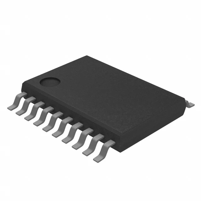
IC CLK/FREQ SYNTH 16TSSOP
- 產品分類
- 時脈產生器、鎖相迴路與頻率合成器
- 封裝
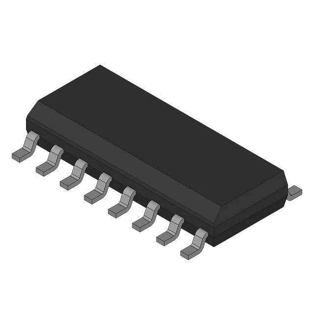
- 16-TSSOP (0.173", 4.40mm Width)
- 庫存
- 2,107 件
- 供貨狀態
- 當前數量需確認。
產品屬性
| 製造商 | Cypress Semiconductor Corp |
|---|---|
| 產品分類 | 時脈產生器、鎖相迴路與頻率合成器 |
| Differential - Input:Output | No/Yes |
| Divider/Multiplier | Yes/No |
| Frequency - Max | 100MHz |
| Input | LVTTL |
| Mounting Type | Surface Mount |
| Number of Circuits | 1 |
| Operating Temperature | 0°C ~ 70°C |
| Output | Clock |
| Package | Bulk |
| PLL | Yes |
| Product status | Active |
| Ratio - Input:Output | 1:2 |
| Supplier Device Package | 16-TSSOP |
| Type | Clock/Frequency Synthesizer, Fanout Distribution, Spread Spectrum Clock Generator |
| Voltage - Supply | 3.135V ~ 3.465V |
| 資料表 | 查看資料表PDF |
採購概覽
CY25823ZZC 的主要供貨及採購資訊。
為何選擇 Antrex Electronics?
為已核實的採購、檢驗及國際採購需求提供獨立分銷支援。
獨立分銷支援
支援短缺、停產及難找電子元器件的生產與採購需求。
可追溯性審查
可在訂單確認前審查標籤、批號、生產批次及現有供應鏈文件。
檢驗與測試
如有需要,可安排外觀檢查、X-ray 及第三方測試支援。
全球採購支援
支援 OEM、EMS、分銷商的國際採購需求,涵蓋單一料號及 BOM 專案。
資質與驗證支援
為電子元器件採購提供品質控制、可追溯性審查及檢驗支援。


CY25823ZZC 詳細描述
Product Overview
The CY25823ZZC from Cypress Semiconductor Corp is a surface-mount clock and frequency synthesizer designed for single-circuit clock generation, fanout distribution, and spread spectrum clock applications. It integrates a PLL, accepts an LVTTL input, and provides clock outputs with a 1:2 input-to-output ratio. The device supports a maximum frequency of 100 MHz and operates from a 3.135 V to 3.465 V supply in a 16-TSSOP package (0.173", 4.40 mm width).
Key Features
- Clock/Frequency Synthesizer with PLL, fanout distribution, and spread spectrum clock generator functionality.
- LVTTL input with differential clock output and 1:2 input-to-output ratio.
- Maximum frequency of 100 MHz in a single-circuit configuration.
- Supply voltage range of 3.135 V to 3.465 V.
- Operating temperature range of 0°C to 70°C.
- Surface-mount 16-TSSOP package, 4.40 mm width.
Applications
- Clock generation and distribution in embedded systems and board-level timing architectures.
- Fanout clock distribution where one input clock feeds multiple downstream logic or interface blocks.
- Spread spectrum clocking in clocked logic subsystems.
Design & Procurement Notes
For layout, verify that the system supply remains within the 3.135 V to 3.465 V range and that the input clock is compatible with LVTTL logic levels. The 1:2 input-to-output ratio and 100 MHz maximum frequency should be checked against the target timing budget. The differential output configuration should be considered when planning board routing and signal pairing. The 0°C to 70°C operating range and 16-TSSOP surface-mount package should be considered when selecting the PCB footprint, thermal path, and enclosure environment.
探索更多採購選項
可按製造商、產品分類或採購需求繼續尋找合適料號。