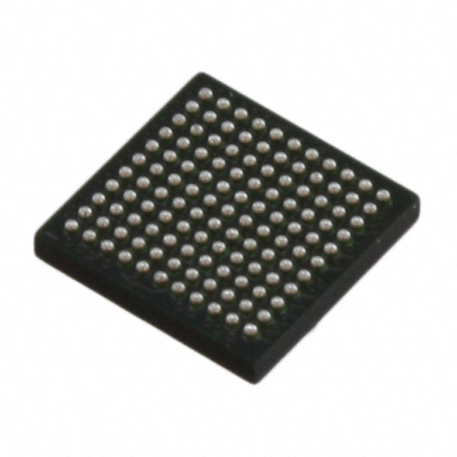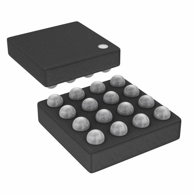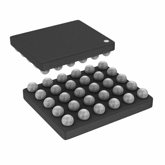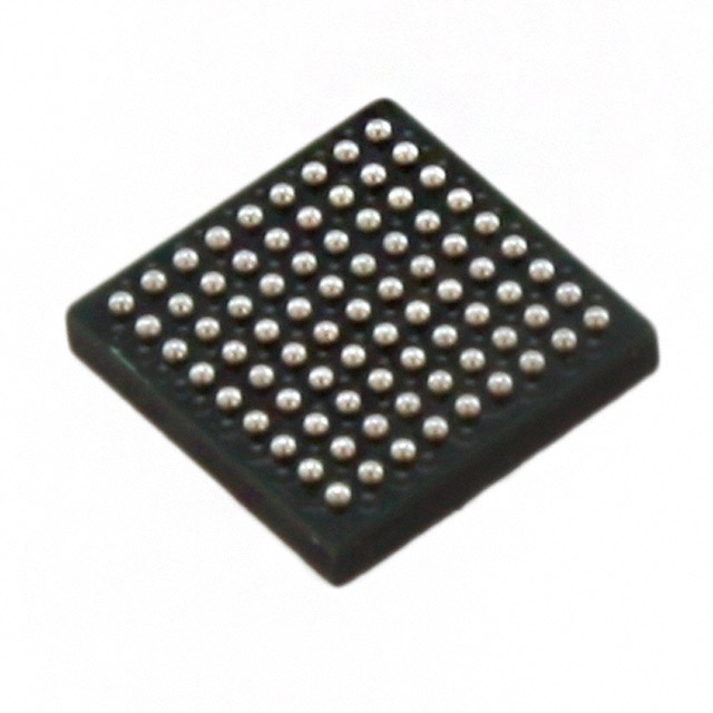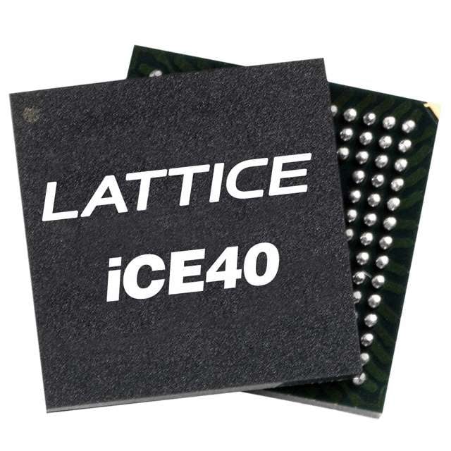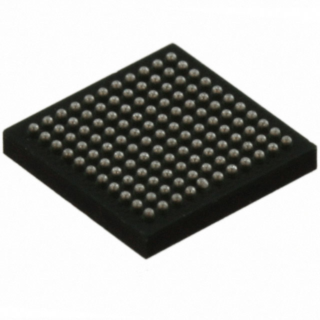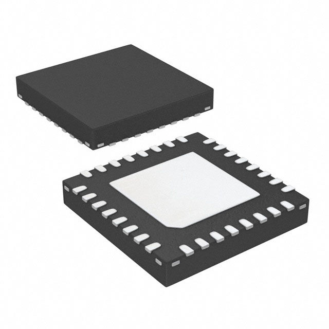
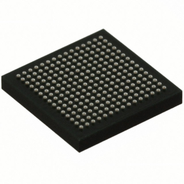
ICE40LP8K-CM225
IC FPGA 178 I/O 225UCBGA
Quick Answer: The ICE40LP8K-CM225 from Lattice Semiconductor Corporation is a field-programmable gate array (FPGA) in the iCE40 LP series, packaged as a 225-VFBGA device with a 225-UCBGA (7x7) package designation.
- Manufacturer
- Lattice Semiconductor Corporation
- Product Category
- FPGA - Field Programmable Gate Array
- Package
- 225-VFBGA
- Stock
- 2,595 pcs
- Availability
- Current quantity subject to confirmation.
Product Attributes
| Manufacturer | Lattice Semiconductor Corporation |
|---|---|
| Product Category | FPGA - Field Programmable Gate Array |
| Mounting Type | Surface Mount |
| Operating Temperature | -40°C ~ 100°C (TJ) |
| Package | Tray |
| Product status | Active |
| Series | iCE40™ LP |
| Supplier Device Package | 225-UCBGA (7x7) |
| Voltage - Supply | 1.14V ~ 1.26V |
| Datasheet | View Datasheet PDF |
Procurement Snapshot
Key supply and purchasing information for ICE40LP8K-CM225.
Why Source from Antrex Electronics?
Independent distribution support for verified sourcing, inspection and international procurement requirements.
Independent Distribution Support
Shortage, obsolete and hard-to-find component sourcing for production and procurement requirements.
Traceability Review
Label, lot, date code and available supply-chain documentation can be reviewed before order confirmation.
Inspection & Testing
Visual inspection, X-ray and third-party testing support can be arranged when required.
Global Procurement Support
Support for OEM, EMS, distributors and international sourcing requirements across individual parts and BOM projects.
Credentials & Verification Support
Quality controls, traceability review and inspection support for electronic component sourcing.


Detailed Description for ICE40LP8K-CM225
Product Overview
The ICE40LP8K-CM225 from Lattice Semiconductor Corporation is a field-programmable gate array (FPGA) in the iCE40 LP series, packaged as a 225-VFBGA device with a 225-UCBGA (7x7) package designation. It provides 7,680 logic elements/cells, 960 LABs/CLBs, 131,072 total RAM bits, and 178 I/O pins for embedded logic and interface expansion. The device operates from a 1.14 V to 1.26 V supply, uses surface-mount assembly, and supports an operating junction temperature range of -40°C to 100°C.
Key Features
- 7,680 logic elements/cells and 960 LABs/CLBs provide configurable digital logic resources.
- 131,072 total RAM bits support on-device data buffering and embedded memory structures.
- 178 I/O pins enable connection to multiple external devices, buses, or interface circuits.
- 1.14 V to 1.26 V supply voltage supports low-voltage embedded board design.
- 225-VFBGA surface-mount package with 225-UCBGA (7x7) package designation and -40°C to 100°C (TJ) operating range.
Applications
- Embedded control systems requiring custom digital logic and multiple I/O interfaces.
- Digital sensor, memory, or peripheral interfacing where 178 I/O pins support diverse external connections.
- Data buffering and signal routing within embedded FPGA-based subsystems.
- Compact surface-mount embedded designs operating from a 1.14 V to 1.26 V supply.
Design & Procurement Notes
Design teams should plan the PCB layout around the 225-VFBGA surface-mount package and the 225-UCBGA (7x7) package designation, including routing for 178 I/O pins and maintaining the supply within 1.14 V to 1.26 V. The 7,680 logic elements/cells, 960 LABs/CLBs, and 131,072 total RAM bits should be compared with the target logic, interface, and buffering requirements before finalizing the architecture. Thermal design should account for the -40°C to 100°C junction operating range, especially when the device is placed in a compact embedded assembly.
Explore More Sourcing Options
Continue sourcing by manufacturer, product category or procurement requirement.