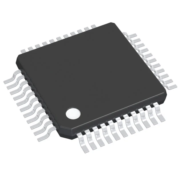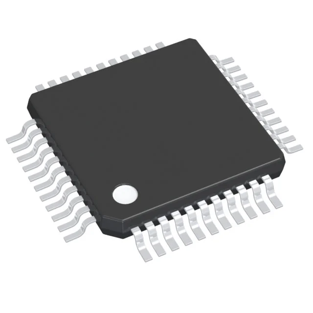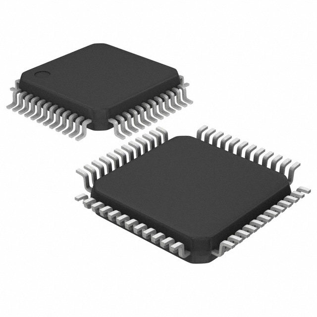
CY9BF364KPMC-G-JNE2
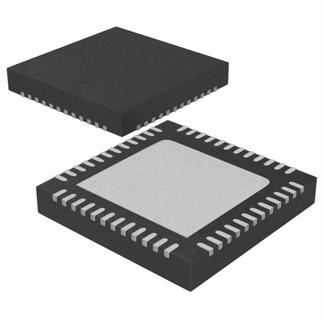
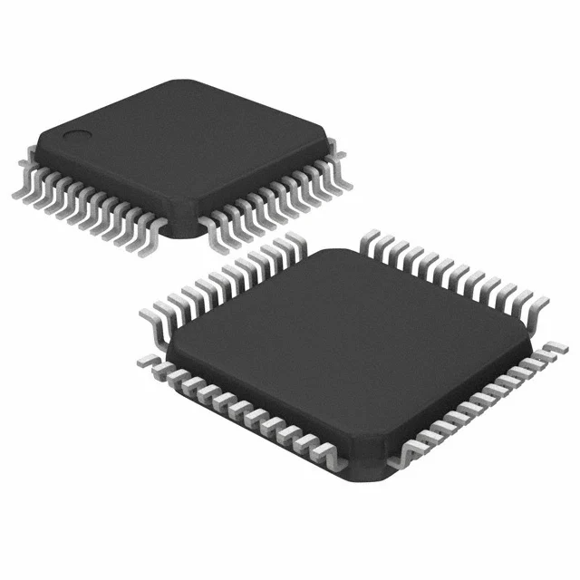
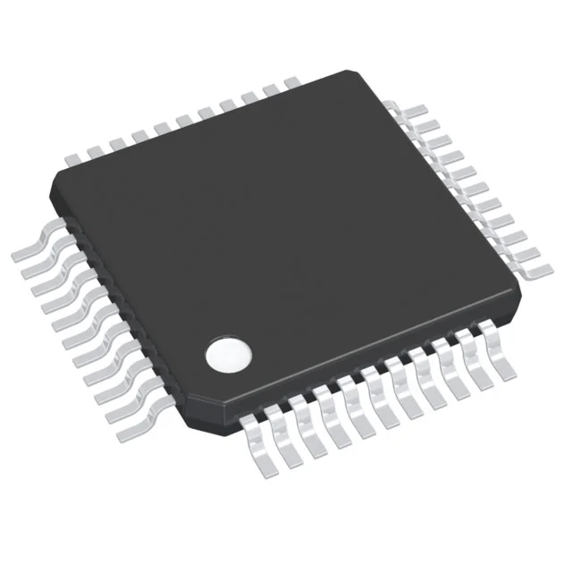
IC MCU 32BIT 288KB FLASH 48LQFP
- 제품 카테고리
- 마이크로 컨트롤러 - MCU
- 패키지
- 48-LQFP
- 재고
- 5,000 개
- 공급 가능 여부
- 현재 수량은 확인이 필요합니다.
제품 특성
| 제조사 | Infineon Technologies |
|---|---|
| 제품 카테고리 | 마이크로 컨트롤러 - MCU |
| Connectivity | CSIO, I2C, LINbus, UART/USART, USB |
| Core Processor | ARM® Cortex®-M4F |
| Core Size | 32-Bit Single-Core |
| Data Converters | A/D 8x12b; D/A 2x12b |
| Mounting Type | Surface Mount |
| Number of I/O | 33 |
| Operating Temperature | -40°C ~ 125°C (TA) |
| Oscillator Type | Internal |
| Package | Tray |
| Peripherals | DMA, LVD, POR, PWM, WDT |
| Product status | Active |
| Program Memory Size | 288KB (288K x 8) |
| Program Memory Type | Flash |
| RAM Size | 32K x 8 |
| Series | FM4 MB9B360L |
| Speed | 160MHz |
| Supplier Device Package | 48-LQFP (7x7) |
| Voltage - Supply (Vcc/Vdd) | 2.7V ~ 5.5V |
| 데이터시트 | 데이터시트 PDF 보기 |
조달 개요
CY9BF364KPMC-G-JNE2의 주요 공급 및 구매 정보입니다.
왜 Antrex Electronics인가요?
검증된 소싱, 검사 및 글로벌 조달 요구에 대해 독립 유통 지원을 제공합니다.
독립 유통 지원
생산 및 조달 요구에 맞춰 수급난, 단종 및 구하기 어려운 전자부품 소싱을 지원합니다.
추적성 검토
주문 확정 전에 라벨, Lot, Date Code 및 제공 가능한 공급망 문서를 검토할 수 있습니다.
검사 및 테스트
필요 시 외관 검사, X-ray 및 제3자 테스트 지원을 진행할 수 있습니다.
글로벌 조달 지원
OEM, EMS 및 유통업체의 국제 조달 요구를 지원하며 단일 부품부터 BOM 프로젝트까지 대응합니다.
인증 및 검증 지원
전자부품 조달을 위한 품질 관리, 추적성 검토 및 검사 지원을 제공합니다.


CY9BF364KPMC-G-JNE2 상세 설명
Product Overview
The CY9BF364KPMC-G-JNE2 from Infineon Technologies is a 32-bit microcontroller built around an ARM® Cortex®-M4F core and operates at 160 MHz. It provides 288 KB of FLASH program memory, 32K x 8 RAM, and 33 general I/O points in a 48-LQFP (7x7) surface-mount package. The device supports a supply range of 2.7 V to 5.5 V and is rated for an operating temperature range of -40°C to 125°C (TA). Connectivity includes CSIO, I2C, LINbus, UART/USART, and USB, while on-chip peripherals include DMA, LVD, POR, PWM, and WDT. Analog resources comprise 8 x 12-bit ADC channels and 2 x 12-bit DAC outputs, and the microcontroller uses an internal oscillator.
Key Features
- 32-bit ARM® Cortex®-M4F core operating at 160 MHz.
- 288 KB FLASH program memory and 32K x 8 RAM.
- 48-LQFP (7x7) surface-mount package with 33 I/O points.
- 2.7 V to 5.5 V supply range and -40°C to 125°C (TA) operating temperature range.
- CSIO, I2C, LINbus, UART/USART, and USB connectivity.
- DMA, LVD, POR, PWM, WDT, internal oscillator, 8 x 12-bit ADC, and 2 x 12-bit DAC.
Applications
- Embedded control modules that combine digital I/O, PWM, and analog measurement.
- Analog sensing or analog output subsystems using 12-bit ADC and 12-bit DAC resources.
- Interface units that use UART/USART, I2C, LINbus, USB, or CSIO.
- Embedded processing subsystems requiring FLASH program storage, RAM, DMA, and supervisory functions.
Design & Procurement Notes
When selecting this part, account for the 48-LQFP surface-mount footprint, 33 available I/O points, and the need to allocate 288 KB FLASH and 32K x 8 RAM for firmware and data. The 2.7 V to 5.5 V supply range should be checked against the system power architecture, while the -40°C to 125°C (TA) range should be checked against board thermal behavior. Designers can plan around the internal oscillator, DMA, PWM, WDT, POR, LVD, and the mixed-signal resources of 8 x 12-bit ADC and 2 x 12-bit DAC. Communication needs should be matched to the device's CSIO, I2C, LINbus, UART/USART, and USB interfaces.
더 많은 소싱 옵션 보기
제조사, 제품 카테고리 또는 조달 요구사항별로 계속 소싱할 수 있습니다.