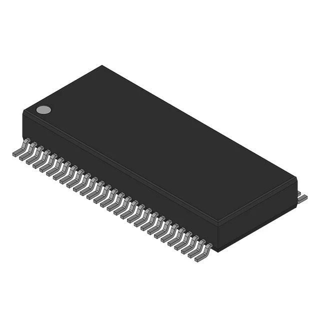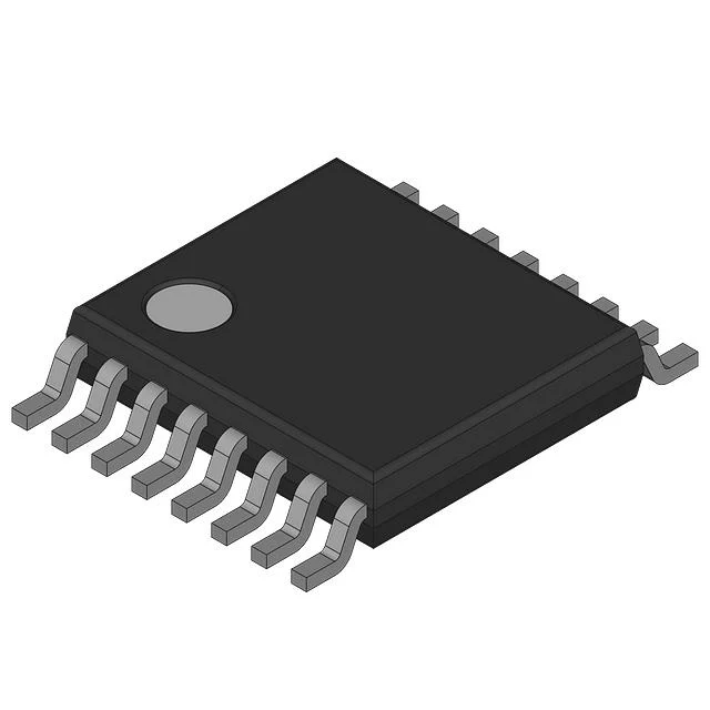
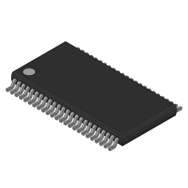
CY2SSTV857ZC-27T
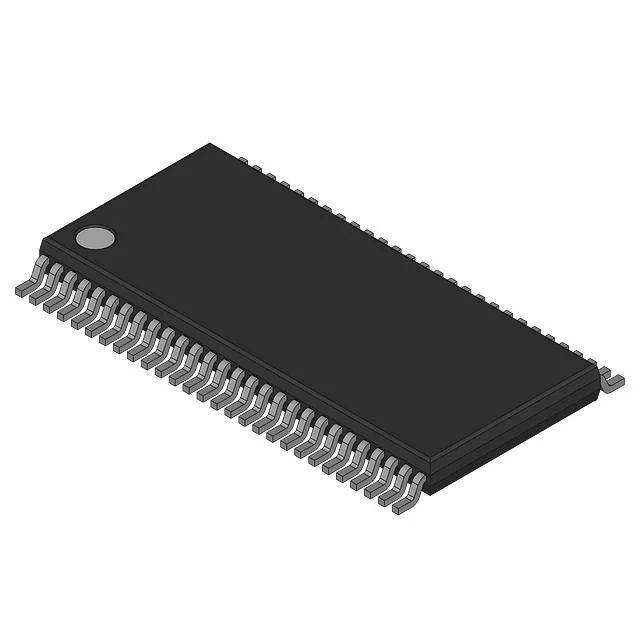
IC CLK ZD BUF 1:10 200MZ 48TSSOP
- 제품 카테고리
- 애플리케이션 특화 클록/타이밍 IC
- 패키지
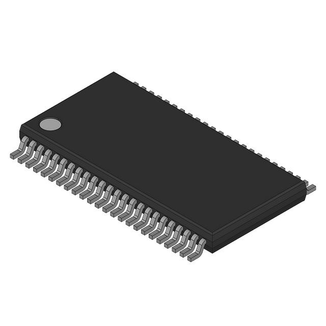
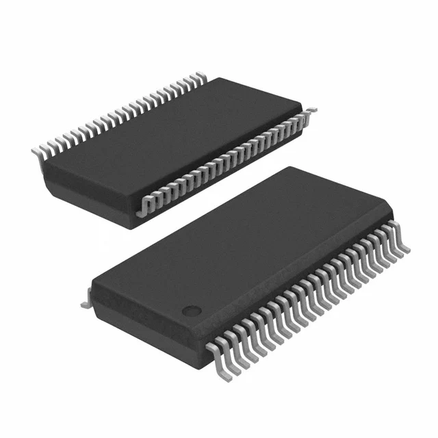
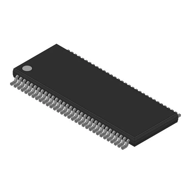
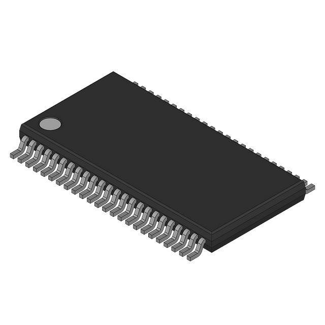
- 48-TFSOP (0.240", 6.10mm Width)
- 재고
- 4,000 개
- 공급 가능 여부
- 현재 수량은 확인이 필요합니다.
제품 특성
| 제조사 | Cypress Semiconductor Corp |
|---|---|
| 제품 카테고리 | 애플리케이션 특화 클록/타이밍 IC |
| Differential - Input:Output | Yes/Yes |
| Input | Clock |
| Mounting Type | Surface Mount |
| Operating Temperature | 0°C ~ 70°C |
| Output | Clock |
| Package | Bulk |
| Product status | Active |
| Ratio - Input:Output | 1:10 |
| Supplier Device Package | 48-TSSOP II |
| Voltage - Supply | 2.38V ~ 2.63V |
| 데이터시트 | 데이터시트 PDF 보기 |
조달 개요
CY2SSTV857ZC-27T의 주요 공급 및 구매 정보입니다.
왜 Antrex Electronics인가요?
검증된 소싱, 검사 및 글로벌 조달 요구에 대해 독립 유통 지원을 제공합니다.
독립 유통 지원
생산 및 조달 요구에 맞춰 수급난, 단종 및 구하기 어려운 전자부품 소싱을 지원합니다.
추적성 검토
주문 확정 전에 라벨, Lot, Date Code 및 제공 가능한 공급망 문서를 검토할 수 있습니다.
검사 및 테스트
필요 시 외관 검사, X-ray 및 제3자 테스트 지원을 진행할 수 있습니다.
글로벌 조달 지원
OEM, EMS 및 유통업체의 국제 조달 요구를 지원하며 단일 부품부터 BOM 프로젝트까지 대응합니다.
인증 및 검증 지원
전자부품 조달을 위한 품질 관리, 추적성 검토 및 검사 지원을 제공합니다.


CY2SSTV857ZC-27T 상세 설명
Product Overview
The CY2SSTV857ZC-27T from Cypress Semiconductor Corp is an Active application-specific clock/timing integrated circuit intended for zero-delay buffering. The device accepts a clock input and provides a clock output with a Ratio - Input:Output of 1:10. Differential operation is available on both the input and output. It operates from a 2.38V to 2.63V supply and is specified for a 0°C to 70°C operating temperature range. The surface-mount package is a 48-TFSOP, 0.240 in / 6.10 mm width, supplied as a 48-TSSOP II device package.
Key Features
- Zero-delay buffer function with a clock input and clock output.
- Ratio - Input:Output of 1:10.
- Differential input and differential output capability is listed for the device.
- Voltage - Supply of 2.38V to 2.63V.
- Operating Temperature of 0°C to 70°C.
- Surface Mount package: 48-TFSOP 0.240 in / 6.10 mm Width, supplier device package 48-TSSOP II.
Applications
- Clock distribution in electronic assemblies that require a buffered clock output from a clock input.
- Timing paths in systems that use differential clock input and differential clock output interfaces.
- Clock buffering in equipment that operates from a 2.38V to 2.63V supply and within 0°C to 70°C.
Design & Procurement Notes
When selecting the CY2SSTV857ZC-27T, confirm that the board supply can maintain 2.38V to 2.63V and that the ambient environment remains within 0°C to 70°C. Verify that the circuit uses differential clock input and differential clock output connections and that the 1:10 input-to-output ratio matches the required clock distribution topology. The 48-TFSOP / 48-TSSOP II surface-mount package should fit the available PCB area. The supplied lifecycle status is Active, which is relevant for current design planning, but final qualification should be checked against the system's environmental and interface requirements.
더 많은 소싱 옵션 보기
제조사, 제품 카테고리 또는 조달 요구사항별로 계속 소싱할 수 있습니다.