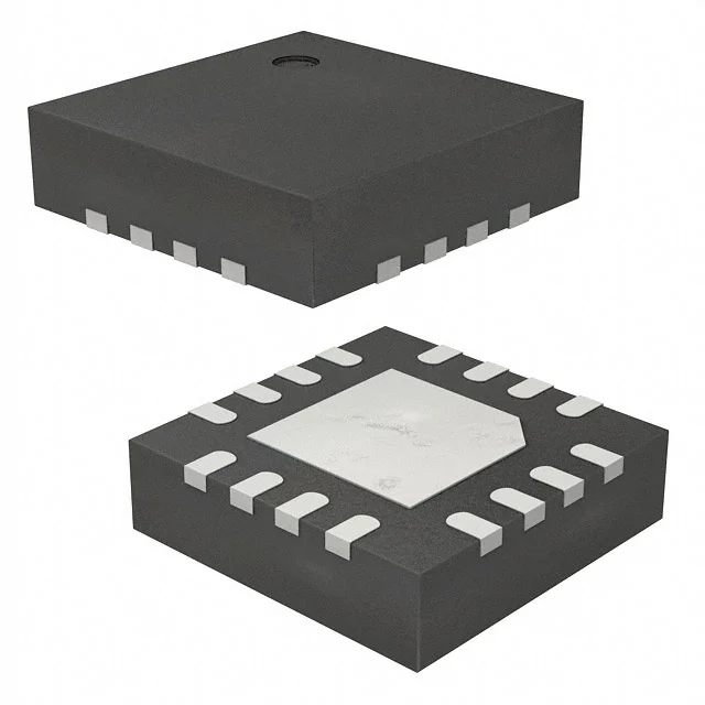
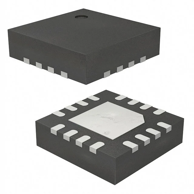
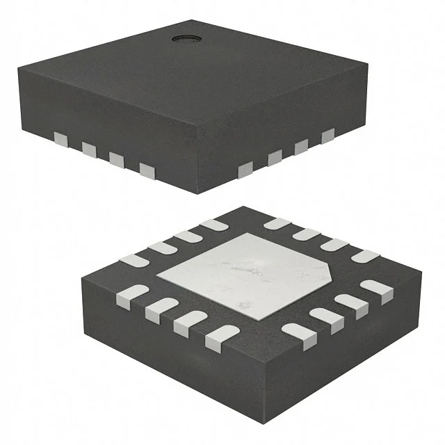
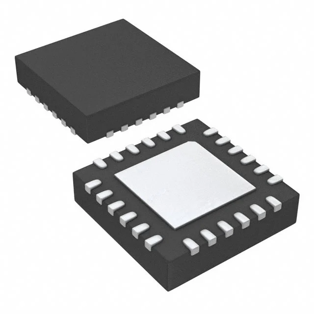
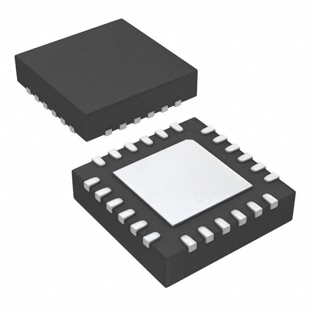
MKL02Z16VFG4R
IC MCU 32BIT 16KB FLASH 16QFN
- メーカー
- NXP USA Inc.
- 製品カテゴリ
- マイクロコントローラ - MCU
- パッケージ
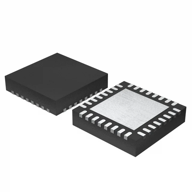
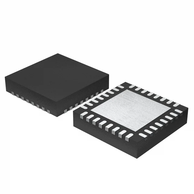
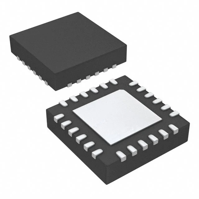
- 16-UFQFN Exposed Pad
- 在庫
- 5,000 pcs
- 供給状況
- 現在の数量は確認が必要です。
製品属性
| メーカー | NXP USA Inc. |
|---|---|
| 製品カテゴリ | マイクロコントローラ - MCU |
| Connectivity | I2C, SPI, UART/USART |
| Core Processor | ARM® Cortex®-M0+ |
| Core Size | 32-Bit Single-Core |
| Data Converters | A/D 6x12b |
| Mounting Type | Surface Mount |
| Number of I/O | 14 |
| Operating Temperature | -40°C ~ 105°C (TA) |
| Oscillator Type | Internal |
| Package | Tape & Reel (TR),Cut Tape (CT) |
| Peripherals | Brown-out Detect/Reset, LVD, POR, PWM, WDT |
| Product status | Active |
| Program Memory Size | 16KB (16K x 8) |
| Program Memory Type | Flash |
| RAM Size | 2K x 8 |
| Series | Kinetis KL02 |
| Speed | 48MHz |
| Supplier Device Package | 16-QFN (3x3) |
| Voltage - Supply (Vcc/Vdd) | 1.71V ~ 3.6V |
| データシート | データシート PDF を表示 |
調達概要
MKL02Z16VFG4R の主要な供給・購買情報です。
Antrex Electronicsを選ぶ理由
確認済みの調達、検査、国際調達要件に対して独立系ディストリビューションのサポートを提供します。
独立系ディストリビューションサポート
生産および調達要件に対応し、供給不足品、製造中止品、入手困難な電子部品の調達を支援します。
トレーサビリティ確認
注文確定前に、ラベル、ロット、デートコード、および利用可能なサプライチェーン書類を確認できます。
検査・試験
必要に応じて、外観検査、X線検査、第三者試験のサポートを手配できます。
グローバル調達サポート
OEM、EMS、ディストリビューターの国際調達要件に対応し、単品部品からBOM案件までサポートします。
認証・検証サポート
電子部品調達向けに品質管理、トレーサビリティ確認、検査サポートを提供します。


MKL02Z16VFG4R の詳細説明
Product Overview
The MKL02Z16VFG4R from NXP USA Inc. is a Kinetis KL02 32-bit microcontroller built around an ARM Cortex-M0+ core and operating at 48MHz. It provides 16KB (16K x 8) of FLASH program memory, 2K x 8 of RAM, and 14 I/O pins in a 16-QFN (3x3) surface-mount package. The device supports I2C, SPI, and UART/USART communication, includes six 12-bit analog-to-digital converter channels, and uses an internal oscillator. Its specified supply voltage range is 1.71V to 3.6V, and the rated ambient operating temperature range is -40°C to 105°C.
Key Features
- 32-bit ARM Cortex-M0+ core with a 48MHz operating speed.
- 16KB (16K x 8) FLASH program memory and 2K x 8 RAM.
- 14 I/O pins with I2C, SPI, and UART/USART serial interfaces.
- Six 12-bit analog-to-digital converter channels for signal measurement.
- Integrated peripherals including brown-out detect/reset, low-voltage detect, power-on reset, PWM, and watchdog timer.
- Internal oscillator and 1.71V to 3.6V supply voltage range.
- 16-QFN (3x3) surface-mount package with 16-UFQFN exposed pad.
Applications
- Compact embedded control systems that require serial communication through I2C, SPI, or UART/USART.
- Analog sensor measurement designs using the 12-bit ADC inputs.
- PWM-based control interfaces for actuators or power stages.
- Surface-mount embedded modules constrained by a 3 mm x 3 mm package footprint.
Design & Procurement Notes
Design and procurement considerations should focus on matching the device to the required memory, I/O, analog, and package constraints. The 16KB FLASH and 2K x 8 RAM should be evaluated against the application code and data footprint, while the 14 I/O pins and six 12-bit ADC channels define the available control and measurement resources. The 1.71V to 3.6V supply range and -40°C to 105°C ambient temperature range should be checked against the system power and environmental requirements. Because the part uses a 16-QFN (3x3) package with an exposed pad, PCB layout, land pattern, and thermal relief should be planned accordingly. The internal oscillator may simplify clock design, but system timing should be verified against the 48MHz core speed and peripheral requirements.
その他の調達オプションを見る
メーカー、製品カテゴリ、または調達要件から引き続き部品をお探しいただけます。