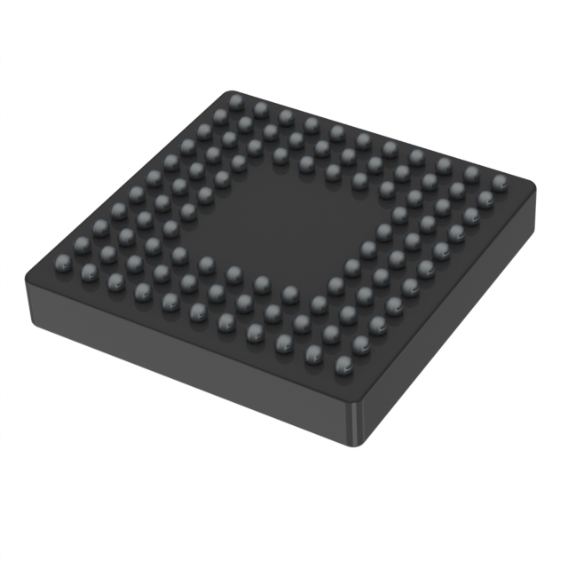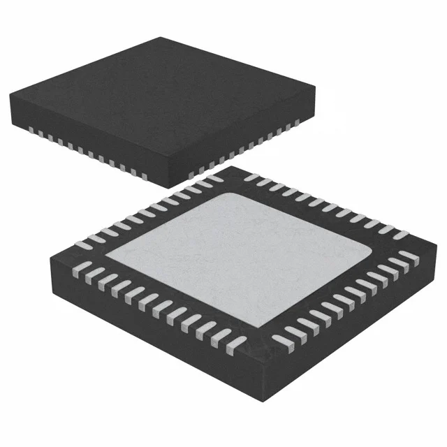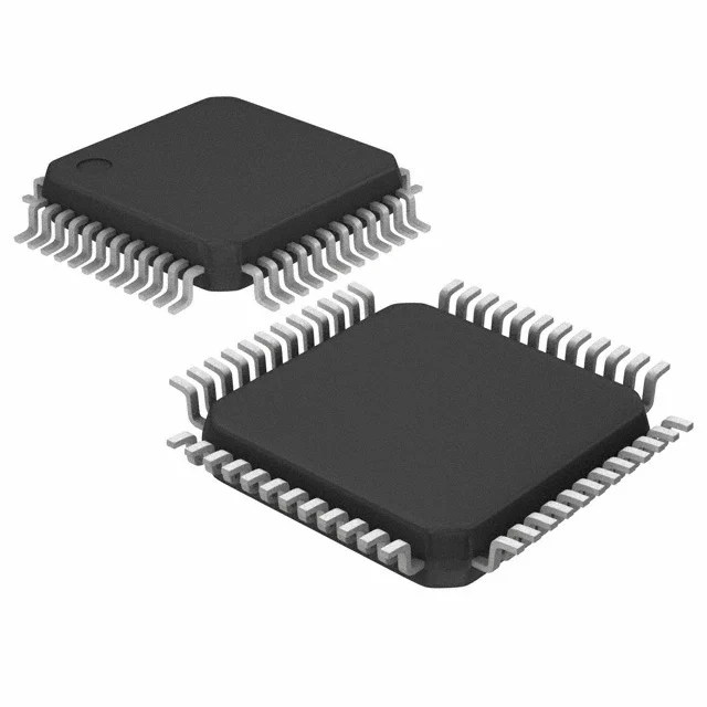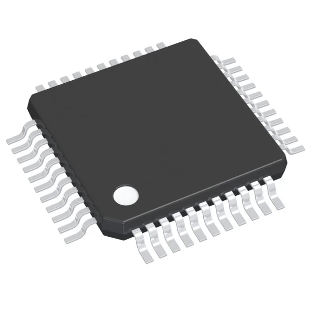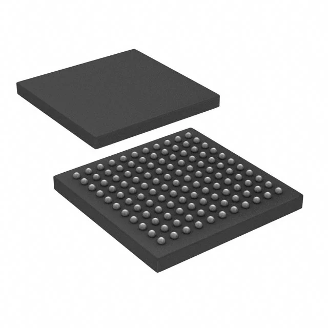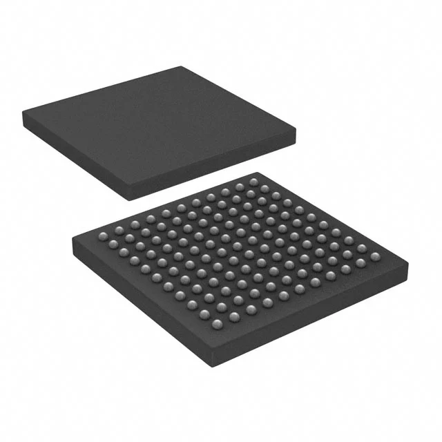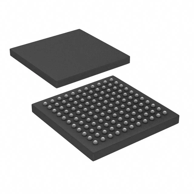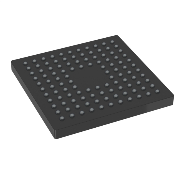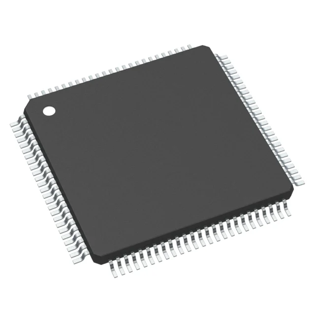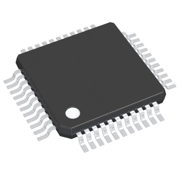
CY9AF112KPMC-G-JNCGE1
IC MCU 32BIT 160KB FLASH 48LQFP
- 製品カテゴリ
- マイクロコントローラ - MCU
- パッケージ
- 48-LQFP
- 在庫
- 2,500 pcs
- 供給状況
- 現在の数量は確認が必要です。
製品属性
| メーカー | Infineon Technologies |
|---|---|
| 製品カテゴリ | マイクロコントローラ - MCU |
| Connectivity | CSIO, I2C, LINbus, UART/USART |
| Core Processor | ARM® Cortex®-M3 |
| Core Size | 32-Bit |
| Data Converters | A/D 8x12b SAR |
| Mounting Type | Surface Mount |
| Number of I/O | 36 |
| Operating Temperature | -40°C ~ 105°C (TA) |
| Oscillator Type | External, Internal |
| Package | Tray |
| Peripherals | DMA, LVD, POR, PWM, WDT |
| Product status | Active |
| Program Memory Size | 160KB (160K x 8) |
| Program Memory Type | Flash |
| RAM Size | 16K x 8 |
| Series | FM3 MB9A110K |
| Speed | 40MHz |
| Supplier Device Package | 48-LQFP (7x7) |
| Voltage - Supply (Vcc/Vdd) | 2.7V ~ 5.5V |
| データシート | データシート PDF を表示 |
調達概要
CY9AF112KPMC-G-JNCGE1 の主要な供給・購買情報です。
Antrex Electronicsを選ぶ理由
確認済みの調達、検査、国際調達要件に対して独立系ディストリビューションのサポートを提供します。
独立系ディストリビューションサポート
生産および調達要件に対応し、供給不足品、製造中止品、入手困難な電子部品の調達を支援します。
トレーサビリティ確認
注文確定前に、ラベル、ロット、デートコード、および利用可能なサプライチェーン書類を確認できます。
検査・試験
必要に応じて、外観検査、X線検査、第三者試験のサポートを手配できます。
グローバル調達サポート
OEM、EMS、ディストリビューターの国際調達要件に対応し、単品部品からBOM案件までサポートします。
認証・検証サポート
電子部品調達向けに品質管理、トレーサビリティ確認、検査サポートを提供します。


CY9AF112KPMC-G-JNCGE1 の詳細説明
Product Overview
The CY9AF112KPMC-G-JNCGE1 is an Infineon Technologies FM3 MB9A110K microcontroller built around a 32-bit ARM Cortex-M3 core operating at 40 MHz. It integrates 160 KB of FLASH program memory, 16 KB of RAM, and 36 I/O pins in a 48-LQFP surface-mount package. The device supports a 2.7 V to 5.5 V supply range and an operating temperature range of -40°C to 105°C. On-chip connectivity includes CSIO, I2C, LINbus, and UART/USART interfaces, while peripheral resources include DMA, low-voltage detection, power-on reset, PWM, and a watchdog timer. An 8-channel 12-bit SAR analog-to-digital converter is available, and oscillator support includes both internal and external options.
Key Features
- 32-bit ARM Cortex-M3 core with 40 MHz operating speed.
- 160 KB FLASH program memory and 16 KB RAM.
- 2.7 V to 5.5 V supply voltage range.
- 36 I/O pins in a 48-LQFP surface-mount package.
- Communication interfaces including CSIO, I2C, LINbus, and UART/USART.
- Peripherals including DMA, LVD, POR, PWM, and WDT.
- 8-channel 12-bit SAR analog-to-digital converter.
- Operating temperature range of -40°C to 105°C.
- Internal and external oscillator support.
Applications
- Embedded control boards that require serial communication through UART/USART, I2C, or CSIO interfaces.
- Sensor and signal acquisition systems using the 8-channel 12-bit SAR ADC for analog measurements.
- PWM-driven actuator or motor-control subsystems within a 2.7 V to 5.5 V supply environment.
- LINbus-based communication modules in embedded networked systems.
- Temperature-sensitive electronic assemblies operating from -40°C to 105°C.
Design & Procurement Notes
When selecting the CY9AF112KPMC-G-JNCGE1, verify that firmware fits within 160 KB FLASH and 16 KB RAM, and that the 40 MHz Cortex-M3 core meets processing requirements. The 2.7 V to 5.5 V supply range and 48-LQFP package affect PCB layout, decoupling, and thermal design. The specified -40°C to 105°C operating range should be considered alongside system-level thermal design. Communication needs should be checked against the available CSIO, I2C, LINbus, and UART/USART interfaces, while analog sensing should be planned around the 8-channel 12-bit SAR ADC. The presence of DMA, LVD, POR, PWM, and WDT can simplify control-loop and reliability functions, but these features require appropriate software configuration.
その他の調達オプションを見る
メーカー、製品カテゴリ、または調達要件から引き続き部品をお探しいただけます。